Table of Contents
Conductor Losses
Conductor losses in a WR187 waveguide primarily arise due to the resistance of the metallic walls that guide electromagnetic waves. These losses are influenced by material properties, frequency, and physical conditions of the waveguide. For instance, copper, a common material for waveguides, has a conductivity of approximately 5.96×10⁷ S/m. For a frequency of 5 GHz, this skin depth for copper is approximately 0.93 micrometers. When the waveguide surface roughness becomes larger than this skin depth, the effective resistance increases and thus the losses increase proportionately. A typical conductor loss for a 1 meter length of WR187 waveguide operating at 4 GHz is approximately 0.02 dB or 0.46% of transmitted power dissipated as heat.
The skin effect provides a strong dependence of conductor losses on the operating frequency: the higher is the frequency, the smaller is the skin depth, and thus the thinner layers on the surface may carry current. For example, at a frequency of 10 GHz, the skin depth in copper is about 0.66 micrometers. In practice, a WR187 waveguide working at 5 GHz with 500 W input power would lose something like 10 W along 10 meters of length. If the frequency is doubled to 10 GHz, the losses can rise by 30%, dissipating nearly 13 W for the same length. This effect shows why high-frequency systems are so concerned with waveguide materials and surface finishes.
Temperature also affects conductor losses. The resistivity of copper increases with temperature at a rate of approximately 0.39% per degree Celsius. In industrial applications where WR187 waveguides are used to transmit microwave energy, a temperature rise from 20°C to 50°C could result in a 12% increase in conductor losses. For example, at 5 GHz, the loss for a copper waveguide might increase from 0.02 dB/m to 0.0225 dB/m over this temperature range. This means that, for a length of 20 m, an extra 5 W will be dissipated in a 1 kW system for every effect introduced by this, which will reduce the overall efficiency.
Material selection and surface treatments greatly affect conductor losses. One more material used for waveguides with lower weight and cost is aluminum at 3.5×10⁷ S/m conductivity; its higher resistivity leads to greater losses compared with copper. For instance, an aluminum-made WR187 waveguide would have 0.03 dB/m loss at 5 GHz that is 6% of power loss at every 10 meters of waveguide length for 1 kW input power. Waveguides are usually silver or gold plated to increase the conductivity and hence reduce the attenuation. As an example, a silver-plated copper waveguide reduces the loss by up to 20% to approximately 0.016 dB/m at 5 GHz:. This can help save up to 8 W over 10 meters for a 500 W system and therefore reduce cost and enhance performance in long-term applications.
Surface Roughness
Surface roughness inside a WR187 waveguide greatly influences the conductor losses since it affects how surface currents flow. At 5 GHz, the skin depth for copper is about 0.93 micrometers. Where this depth is shallow compared to the surface roughness, the effective resistance increases since the current is obliged to navigate a tortuous path, leading to increased energy dissipation. For instance, a waveguide with a surface roughness of 0.5 micrometers may incur a loss of 0.02 dB/m. When the roughness increases to 1.5 micrometers, the losses can almost double to 0.04 dB/m. Over a 10-meter length, this could result in the dissipation of 9 W out of a 500 W system and so requires very smooth surfaces.
At still higher frequencies, the roughness in the surface becomes even more critical. For the WR187 waveguide operating at 10 GHz, the skin depth in copper is reduced to about 0.66 micrometers. If the roughness stays at 0.5 micrometer level, the rise in resistance is negligible. However, the roughness rises to 1 micrometer, which is well above the skin depth, and the rise in conductor losses becomes very large. Attenuation may increase from 0.03 dB/m to 0.06 dB/m and power loss will almost be doubled. With a 1-kW input system, for example, such an increase over 15 meters of waveguide would imply approximately an additional 30-W loss. This is how even very modest changes in surface texture can become highly important at high frequencies.
The surface roughness effects are further accentuated by imperfections like machining marks, corrosion, or deposits. In industrial waveguides exposed to harsh environments, surface degradation can lead to losses far exceeding those observed in pristine conditions. For example, in an aged WR187 waveguide with a roughness averaging 2 micrometers, losses at 5 GHz can reach 0.05 dB/m. Over a 20-meter length, this would translate to an overall loss of 100 W in a 1 kW system, while a new, well-polished waveguide with 0.5 micrometers roughness loses only 40 W. These differences put a big emphasis on regular inspection and maintenance if performance has to be kept within acceptable limits.
Frequency of Operation
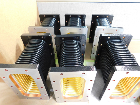
Losses in the WR187 waveguide are greatly influenced by the frequency of operation, due to the influence of skin depth and thus attenuation of power. The skin depth in copper at 4 GHz, which is typically within the range of the WR187, is around 1 micrometer. It defines the distance down to which the induced current propagates in the waveguide walls. At this frequency, the conductor loss is approximately 0.02 dB/m. For a 10-meter waveguide carrying 1 kW of input power, this amounts to a power loss of approximately 46 W, leaving 954 W being delivered to the load.
With increased frequency, the skin depth becomes smaller. This would result in a higher effective resistance in the waveguide walls. For example, at 8 GHz, the skin depth for copper decreases to around 0.66 micrometers. The lesser penetration increases current density at the surface, which in turn amplifies the resistive losses. For the same WR187 waveguide, the conductor loss increases to approximately 0.035 dB/m at 8 GHz. For a path length of 10 meters with an input power of 1 kW, the loss increases to 79 W, where the transmitted power will now be 921 W. This clearly shows that as frequency increases, there is higher attenuation; hence, the materials and waveguide must be chosen and designed correctly.
Frequency also affects other types of losses, like mode conversion and dielectric interactions. Within the operating frequency range, the dominant TE10 mode is well confined within the WR187 waveguide, thus unwanted mode conversion is minimized. However, near the upper limit of the WR187 frequency range of approximately 8.2 GHz, higher-order modes may be excited owing to imperfections or bends in the waveguide and add further losses. For example, a waveguide bend at 8 GHz may introduce an additional loss of 0.02 dB and increase the total attenuation of a 10-meter system by about 20%. That is, approximately another 20 W of power can be dissipated on top of the normal conductor losses to further impact the efficiency.
Dielectric Loss
One other form of dielectric loss in a WR187 waveguide involves energy absorption from the field by an insulating material, usually, within the waveguide. The magnitude of this usually depends on the loss tangent (tan δ) and the dielectric constant (εr) of the dielectric material. A commonly used dielectric such as PTFE, for example, with a dielectric constant of 2.1 and a loss tangent of 0.0002, introduces about 0.01 dB/m loss at 5 GHz. Over a 10-meter length, this equates to some 2.3 W total dissipated power for a 500 W system.
Frequency of operation increases the dielectric losses because of the frequency dependency of the loss tangent. For example, at 5 GHz, a dielectric material having a loss tangent of 0.001 contributes some 0.05 dB/m in a WR187 waveguide. Whereas if the frequency were to go up to 7 GHz, due to increased interaction between the electromagnetic field and the dielectric medium, the material’s loss may go up to 0.07 dB/m. The extra loss in a 10-meter waveguide carrying an input power of 1 kW compared to its operation at 5 GHz is 20 W; this largely reduces efficiency in high-power applications.
The thickness and position of the dielectric material determine the losses. In several cases, dielectric slabs are inserted into the waveguide to support some component or to guide certain modes. For instance, a 1-mm-thick slab of quartz (dielectric constant 3.8, loss tangent 0.0004) placed centrally in a WR187 waveguide at 6 GHz can introduce additional loss of 0.03 dB/m. Over an extent of 5 meters in waveguide, this slab can dissipate 7.5 W out of an input signal of 500 W. Very significant and thus sensitive to material choice and positioning.
Impedance Mismatch
Impedance mismatch in a WR187 waveguide arises when the characteristic impedance of the waveguide does not match those from other connected components, such as antennas, transitions, or terminations. Such a mismatch results in part of the power that is transmitted being reflected back toward the source. This lessens the efficiency in power transfer. For example, at 5 GHz, the characteristic impedance of a WR187 waveguide is approximately 470 ohms. For the same antenna, if the impedance of the connected load is 400 ohms, then the VSWR becomes 1.175 and the reflection coefficient is 0.08. Power reflected in this case becomes 0.64%. If the input power is 1 kW then the mismatch reflects 6.4 W of power back to the source.
When impedance mismatch is more significant, losses increase exponentially. For example, if the impedance of the load decreases to 300 ohms, then the VSWR increases to 1.57 and the coefficient of reflection becomes 0.22. The reflected power becomes 4.8%. On a 500 W system, that would be 24 W of the power being reflected, hence only 476 W of power delivered. This also promotes standing waves within the waveguide that can cause localised hotspots, potentially damaging the waveguide or other attached components.
Frequency is a critical factor in impedance mismatch. As frequency increases, even slight physical imperfections or changes in the geometry of components may cause greater mismatches. For example, a waveguide section operating at 5 GHz with a 10% mismatch in impedance might have a reflection coefficient of 0.1, resulting in a power loss of 1%. If the frequency increases to 7 GHz, the same physical mismatch could lead to a reflection coefficient of 0.15, reflecting 2.25% of the power. This added reflection at higher frequencies for a 10-meter WR187 waveguide with 1 kW input power could result in an additional 12.5 W of power reflecting back toward the source.
Leakage Loss
The leakage loss in the WR187 waveguide is considered to be that electromagnetic energy that escapes through imperfect connections, seams, or structural flaws. This kind of loss depends on the quality of waveguide assembly and frequency of operation. For instance, at 5 GHz, a typical WR187 waveguide system with well-sealed flanges may experience a leakage loss of less than 0.01 dB per joint. However, if due to poor alignment there is a gap of 0.1 mm between flanges, it may increase the loss up to 0.1 dB per joint, with an additional power loss of 2.3 W in a system transferring power at 500 W over five joints.
Increased leakage losses occur at higher frequencies since higher frequencies are more sensitive to imperfections. At a frequency of 7 GHz, the same 0.1 mm gap between flanges will give about 0.15 dB loss per joint. In systems with 10 joints along a 20-meter waveguide, there would be a combined leakage loss of about 1.5 dB. That is, the power in a 1 kW transmission would be reduced by approximately 20%. This implies that there is a leakage loss of 200 W of power, demonstrating how waveguide assembly and maintenance are to be handled accurately, particularly in high-frequency systems.
Seam quality is one of the major contributors to leakage loss. For example, a poorly welded seam or small cracks on a portion of a WR187 waveguide will result in significant energy leakage. A 1-meter segment with a single 0.2 mm crack can face up to 0.05 dB loss at 5 GHz. With several sections, the same path may lead to an accumulated effect reaching 0.75 dB in a 15-meter waveguide. This accounts for 15% power loss within a 1 kW system. Regular inspection and use of high-quality welding techniques avoid such things because any leak would be reduced to a minimum.
Bend and Junction Losses
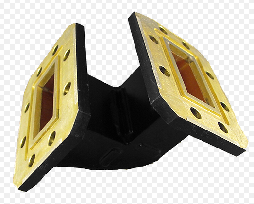
Bend and junction losses in a WR187 waveguide occur when the direction of the geometry of the waveguide changes or at the junctions where more than one waveguide sections connect. This produces energy scattering and mode conversion. For a single 90-degree bend with a radius of 2 times the waveguide width (2a) the loss at 5 GHz is typically around 0.02 dB. In a 10-meter waveguide with three such bends, the cumulative bend loss would be approximately 0.06 dB, leading to a power dissipation of 6.9 W in a 1 kW system. Increasing the bend radius to 3a can reduce the loss per bend to about 0.01 dB, cutting the cumulative loss in half.
At higher frequencies, bend losses become more significant due to shorter wavelengths and increased sensitivity to geometric changes. As an example, a 90-degree bend having a radius of 2a will have a loss of approximately 0.03 dB/bend at 8 GHz. On a 20-meter waveguide with five bends, the total bend loss can go to 0.15 dB and, correspondingly, for a 500 W system, this means a reduction of about 15.5 W of power. This loss can be reduced by optimizing the bend radius and making smooth transitions, which allows a better transmission efficiency for higher operating frequencies.
Junction losses occur at connections of waveguide sections with flanges, T-junctions, or couplers. A standard flange connection with good alignment introduces an insignificantly small loss, less than 0.01 dB at 5 GHz. However, a misaligned junction with a 0.1 mm offset may introduce a loss as high as 0.05 dB per connection. For a system with 10 junctions on a 15-meter waveguide, this amounts to an overall loss of 0.5 dB at the expense of 11.3 W in a 1 kW system. It is possible to reduce these losses and thereby improve the performance of the system by using precision alignment tools and machining.

