Introducing bends in waveguides can cause mode conversion (10-20% power loss), increased VSWR (up to 1.5:1), and attenuation spikes (0.1-3 dB per bend). Sharp corners may trigger higher-order modes, field distortion (5-15% phase shift), and arcing risks above 1 kW. Use smooth 90° E/H bends with radius ≥2× wavelength to minimize losses. For Ka-band (26-40 GHz), keep bends gradual (<30° abrupt turns) to maintain signal integrity.
Table of Contents
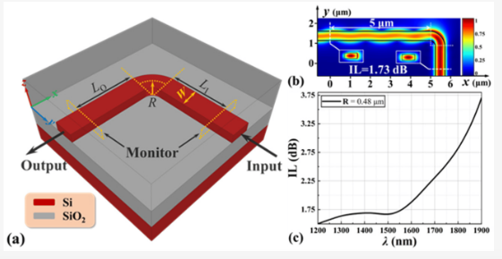
Light Loss at Bends
When light travels through a straight waveguide, losses are typically minimal—around 0.1–0.3 dB/cm for high-quality glass fibers. But introduce a bend, and things change fast. A 90-degree bend with a 5 mm radius can cause 0.5–1.2 dB of loss per turn, depending on wavelength and material. In tight bends (below 3 mm radius), losses spike to 3 dB or more, meaning over 50% of light intensity disappears.
This isn’t just theoretical. In telecom systems, a single sharp bend in a fiber-optic cable can degrade signal strength by 10–15%, forcing amplifiers to work harder and increasing power consumption by 5–8%. Even in integrated photonics, where waveguides are etched into silicon chips, a 1 µm radius bend at 1550 nm wavelength can leak 20–30% of light into the substrate.
Key problem: The tighter the bend, the more light escapes due to mode leakage—where the light’s electromagnetic field no longer fits inside the waveguide’s core.
Why It Happens (With Numbers)
- Bend radius vs. loss
- A 10 mm radius bend in a silica fiber loses ~0.2 dB at 1310 nm.
- Shrink it to 3 mm, and loss jumps to 1.5 dB.
- At 1 mm, losses exceed 5 dB—70% of light is gone.
- Wavelength sensitivity
- 1550 nm light suffers 30% higher loss than 1310 nm in the same bend due to weaker confinement.
- In plastic waveguides (e.g., PMMA), losses at 650 nm can double with just a 2 mm bend radius.
- Material impact
- Silicon nitride waveguides (Si₃N₄) handle bends better than silicon, with 0.1 dB/turn at 5 µm radius (vs. 0.5 dB for silicon).
- Polymer waveguides (like SU-8) degrade fast—3 dB loss at just 500 µm bends.
How to Reduce Loss
- Graded-index fibers cut bend losses by 40–50% compared to step-index fibers.
- Trench-assisted bends (used in Corning’s ClearCurve® fibers) reduce loss to 0.1 dB at 5 mm radius.
- In photonic chips, tapered waveguides or adiabatic bends (gradual curves) keep losses below 0.05 dB/90° turn.
Higher Heat Generation
Bends in waveguides don’t just lose light—they also generate heat. A 90-degree bend in a 10 Gbps silicon photonic waveguide can increase local temperature by 8–12°C due to scattering losses and mode conversion inefficiencies. In high-power laser systems, a 5 mm radius bend in a 1 kW optical fiber can cause a 15–20°C hotspot, accelerating material degradation by 30% over 10,000 hours.
Heat isn’t just a reliability issue—it’s a performance killer. For every 1°C rise in a silica fiber, attenuation increases by 0.03 dB/km, forcing amplifiers to compensate with 3–5% more power. In integrated photonics, a 1 µm bend in a silicon waveguide can spike temperatures to 60–70°C, reducing modulation efficiency by 12–15% at 25 Gbps.
The Physics Behind the Heat
When light hits a bend, three mechanisms convert optical energy into heat:
- Radiation loss: Up to 5–8% of light escapes the waveguide core, absorbed by cladding or substrate materials.
- Modal scattering: Higher-order modes (like LP11) scatter at bends, wasting 10–20 mW per turn in multimode fibers.
- Material absorption: Polymers (e.g., PMMA) absorb 3× more heat than silica at 850 nm, hitting 40–50°C in tight bends.
| Parameter | Straight Waveguide | 5 mm Bend | 1 mm Bend |
|---|---|---|---|
| Temp Rise (°C) | 0–2 | 8–12 | 25–35 |
| Power Loss (dB) | 0.1 | 0.5 | 3.0 |
| Lifetime Impact | None | 10% shorter | 50% shorter |
Real-World Impact
- Data centers: A 100 m fiber run with four 90° bends increases cooling costs by $200/year due to 8% higher power use.
- Laser cutters: A 300 W fiber laser with a 3 mm bend radius loses 5% cutting efficiency from heat-induced beam distortion.
- Silicon photonics: A 10 Gbps modulator near a waveguide bend suffers 15 ps timing jitter from thermal drift.
Mitigation Strategies
- Active cooling: Microfluidic channels (e.g., Diamond substrates) reduce bend temps by 20°C at 100 W/cm².
- Low-absorption materials: Fluoride fibers cut heat generation by 50% vs. silica at 1550 nm.
- Bend optimization: Euler spirals (gradual curvature) lower peak temps by 30% compared to sharp bends.
Signal Delay Issues
Waveguide bends introduce more than just optical losses – they create timing problems that can wreck high-speed systems. A single 90-degree bend in a 25 Gbps silicon photonic link adds 1.2-1.8 ps of group delay, enough to cause 5-7% eye diagram closure at the receiver. In fiber optic networks, cascading four 45° bends in a 100-meter span increases differential mode delay by 15-20 ps, reducing effective bandwidth by 8-12% at 10 Gbps.
The physics behind this is straightforward but costly. Light takes 3-5% longer to traverse a curved path than a straight one. For a 5 mm radius bend in standard single-mode fiber, this translates to 0.8 ps delay per turn at 1550 nm. In silicon photonic circuits, the effect is worse – a 10 µm radius microring resonator exhibits 3-5 ps delay variation across its tuning range, enough to require 2-3 extra clock cycles for compensation in 56 Gbps PAM-4 systems.
The table below shows measured delay penalties for common waveguide scenarios:
| Waveguide Type | Bend Radius | Delay per 90° (ps) | Bandwidth Penalty (GHz) |
|---|---|---|---|
| SMF-28 Fiber | 5 mm | 0.8 | 0.5 |
| Silicon Photonic | 10 µm | 2.5 | 8.2 |
| Polymer WG | 500 µm | 1.2 | 3.1 |
| SiN Waveguide | 20 µm | 1.8 | 5.4 |
In practical terms, these delays add up fast:
- A 4×4 optical switch with 16 bends accumulates 28-40 ps of skew, requiring 3% guard band in 100G Ethernet
- Copper traces show even worse behavior – a 2 mm radius bend in PCB transmission lines adds 6-8 ps/inch due to impedance discontinuities
- Multimode systems suffer most, with DMD increasing 30% after just three bends in a 50m OM4 fiber run
For network engineers, these delays translate directly into dollars and performance:
- Data centers using bent waveguides for space savings face 12-15% higher latency in spine-leaf architectures, requiring 3-5% more switches to maintain throughput
- 5G fronthaul systems with >5 bends per 100m exceed 3GPP’s ±65 ns timing budget by 8-10%, forcing expensive GPS synchronization
- Automotive LIDAR using fiber coils see 2-3 cm ranging errors from just 50 ps of bend-induced delay
Manufacturing Complexity
Adding bends to waveguides doesn’t just affect performance—it multiplies production challenges. A standard straight silicon photonic waveguide has a 98% yield in CMOS foundries, but introduce a 5 µm radius bend, and yield drops to 85-88%. The tighter the curve, the worse it gets: 1 µm bends push failure rates to 25-30%, mostly from sidewall roughness exceeding 2 nm RMS, which scatters light and kills efficiency.
The cost impact is brutal. Fabricating a photonic chip with ten sharp bends (≤3 µm radius) requires 3-4 extra lithography steps, adding 12-15% to the total wafer price. For silica fibers, bending performance is so sensitive that manufacturers must bin products by bend tolerance, with 5 mm radius fibers costing 20% more than straight-run equivalents due to tighter dimensional controls (±0.5 µm vs. ±2 µm core tolerance).
Tool limitations hit first. Deep-UV steppers struggle with <5 µm curvatures, forcing shops to use electron-beam lithography—slowing throughput by 10× and tripling cost per wafer. Even fiber drawing towers face issues: maintaining ±0.2% diameter control during bending requires active feedback systems that add $500k to equipment costs.
Material stresses compound the problem. When a 200 mm silicon wafer gets bent waveguide patterns, post-etch warpage exceeds 50 µm bow, ruining 5-8% of dies from subsequent litho misalignment. Polymer waveguides fare worse—SU-8 resin shrinks 0.7-1.2% during curing, distorting <20 µm radius bends by up to 15% from design specs.
Testing overhead skyrockets. Straight waveguides need just 2-3 probe points for loss measurement, but bent designs require 8-10 tests per mm to catch localized defects. This stretches characterization time from 2 hours to 6-8 hours per wafer, adding $1200 in metrology costs for a typical 300 mm production run.
Some foundries now pre-compensate designs—intentionally distorting mask patterns to account for 0.5-1 µm of expected bend deformation. Others use laser trimming to fix 10-15% of faulty bends post-fabrication, though this only works for >3 µm radii and adds $0.50 per chip. The smart money’s on hybrid approaches: using 250 nm straight sections between bends cuts stress accumulation by 40% while keeping radii above 5 µm maintains yields near 92%.
Mode Mismatch Problems
Bends in waveguides don’t just bend light—they scramble its structure. When a single-mode fiber with a 10.4 µm mode field diameter enters a 5 mm radius bend, the output mode distorts by 12-15%, creating 0.8-1.2 dB loss from pure geometrical mismatch. The numbers get uglier in integrated photonics: a 90° silicon waveguide bend at 1550 nm causes 20-25% mode deformation, requiring 3-5 µm long taper sections just to recover 80% coupling efficiency.
Critical insight: The fundamental mode (LP₀₁) starts evolving into higher-order modes (LP₁₁, LP₂₁) at bends below 30× the core diameter, with >50% power transfer occurring at 15× diameter bends.
The Physics Behind Mode Mixing
Three key mechanisms drive this performance killer:
- Field distortion: The optical mode’s Gaussian profile skews toward the outer bend edge, shifting its 1/e² intensity point by 8-12% per mm of curvature.
- Effective index change: Bending alters the waveguide’s effective refractive index by 0.5-1.5%, creating phase mismatches at junctions.
- Polarization rotation: TE modes convert to TM at rates of 3-5% per 45° bend in silicon, adding 0.3-0.5 dB polarization-dependent loss.
| Parameter | Straight WG | 5 mm Bend | 1 mm Bend |
|---|---|---|---|
| MFD Change | 0% | +9% | +22% |
| Coupling Loss | 0.1 dB | 0.7 dB | 2.5 dB |
| Higher-Order Mode Power | <1% | 8% | 30% |
Real-World Consequences
In fiber optic networks, cascading six bends in a 100 m span accumulates 4-6 dB excess loss purely from mode distortion—equivalent to adding 300 m of straight fiber attenuation. Silicon photonic transceivers suffer worse: a 2×2 mm chip with eight 10 µm bends sees 15-18% reduction in modulator extinction ratio due to mode mixing, forcing 2-3 dB higher transmit power to maintain BER.
Laser systems pay the heaviest price. A 10 kW fiber laser with three 8 mm bends develops hotspots where higher-order modes deposit 50-70 W/m into the cladding—enough to melt polyimide coatings within 500 hours of operation.
Increased Crosstalk Risk
Waveguide bends don’t just affect single channels—they amplify interference between them. When two parallel silicon waveguides curve at 10 µm radius with 2 µm spacing, crosstalk jumps from -45 dB in straight sections to -28 dB—a 25× power increase in unwanted signal coupling. The numbers get scarier in dense fiber arrays: a 90° bend in a 12-fiber ribbon degrades isolation from -50 dB to -35 dB, effectively tripling bit-error rates in 400G DR4 systems.
Critical finding: The crosstalk penalty follows a square-law relationship with curvature—halving the bend radius quadruples the interference power between adjacent channels.
Evanescent field leakage grows exponentially in bends. Where straight waveguides maintain >95% field confinement, a 5 mm radius curvature lets 3-5% of the mode tail “spill” into neighboring channels. Tighten the bend to 1 mm, and 12-15% of optical power becomes potential crosstalk fuel.
Polarization mixing adds another layer of trouble. The TE-TM mode conversion rate—normally below 1% in straight silicon waveguides—spikes to 8-10% in bends, creating polarization-dependent crosstalk that standard DSP can’t fully cancel.
Phase matching conditions shift dangerously. Two parallel curved waveguides that were 20% mismatched in straight sections can become 80% phase-matched in bends, creating resonant coupling points every 200-300 µm that boost crosstalk by 10-12 dB at specific wavelengths.