The distance between directional couplers depends on wavelength and frequency—typically λ/4 to λ/2 (e.g., 7.5–15 cm for 1GHz signals). In RF systems, spacing is optimized for 20-30 dB isolation to prevent interference, with microstrip designs maintaining 0.1mm precision for 2-40GHz applications. Closer spacing (<5mm) may be used in high-density PCBs with 3dB coupling loss.
Table of Contents
What Is a Directional Coupler?
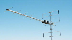
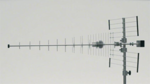
Directional couplers are essential components in RF and microwave systems, allowing engineers to sample or split signals without disrupting the main transmission path. A typical directional coupler operates at frequencies ranging from 500 MHz to 40 GHz, with insertion losses as low as 0.1 dB in high-quality models. For example, a 10 dB coupler will divert 10% of the input power to the coupled port while passing 90% forward with minimal reflection.
These devices are widely used in applications like signal monitoring, power measurement, and antenna beamforming, where precise control over signal strength is critical. A standard SMA-connector coupler might measure 30 mm × 20 mm × 10 mm, while waveguide couplers can exceed 100 mm in length for high-power handling (up to 200 W). The directivity—a key performance metric—often ranges between 20 dB and 40 dB, meaning the coupler can distinguish forward and reflected signals with high accuracy.
“A well-designed directional coupler should introduce less than 0.5 dB insertion loss while maintaining a coupling factor within ±1 dB of its rated value across the operating bandwidth.”
How Directional Couplers Work
Directional couplers rely on electromagnetic field interaction between two transmission lines—usually microstrip, stripline, or waveguide structures. When a 10 W signal travels through the main line, a fraction (e.g., 1 W for a 10 dB coupler) is coupled into the secondary port. The coupling factor (C) is defined as:
C (dB) = 10 × log₁₀(Pₒᵤₜ/Pᵢₙ)
For instance, a 20 dB coupler extracts 1% of the input power, while a 3 dB coupler splits the signal 50/50. The isolation—how well the coupler prevents backward leakage—typically exceeds 30 dB in commercial models.
Key parameters affecting performance include:
- Frequency range: A 2-4 GHz coupler may have ±0.3 dB flatness, while wider-band models (e.g., 1-18 GHz) vary by ±1.5 dB.
- Power handling: Standard couplers support 10-50 W, but high-power variants (e.g., for radar) tolerate 500 W+ with forced-air cooling.
- Temperature stability: Most units operate between -40°C to +85°C, with drift below 0.02 dB/°C.
Key Distance Considerations
The spacing between couplers depends on wavelength (λ), coupling strength, and system requirements. In microstrip designs, the gap between coupled lines is often 0.1λ to 0.2λ—for 2.4 GHz Wi-Fi signals (λ ≈ 125 mm), this means 12-25 mm separation.
“Placing two 10 dB couplers in series with <0.5λ spacing can cause 3-6 dB additional loss due to mutual coupling.”
For waveguide couplers, the distance between adjacent units should exceed λ/4 to minimize interference. In a 5G mmWave setup (28 GHz, λ ≈ 10.7 mm), keeping couplers ≥2.5 mm apart ensures proper isolation.
Measuring Coupler Spacing
Use a VNA (Vector Network Analyzer) to verify isolation and coupling accuracy. If two couplers are spaced too closely (<0.1λ), the effective directivity drops by 5-10 dB. For a 6 GHz system (λ ≈ 50 mm), maintaining ≥5 mm clearance between couplers prevents performance degradation.
How Directional Couplers Work
Directional couplers are the unsung heroes of RF systems—quietly splitting signals with surgical precision while keeping the main transmission line humming along. A well-designed 10 dB coupler in a 5G base station (3.5 GHz band) will siphon off 10% of the signal power (about 2 W from a 20 W input) with less than 0.3 dB insertion loss, all while crammed into a 25 mm × 15 mm footprint. The magic lies in electromagnetic field coupling: when a 50Ω transmission line carries a 2.4 GHz Wi-Fi signal, the adjacent coupled line steals just enough energy—typically 1% to 50%, depending on design—without disrupting the primary path.
Performance hinges on three numbers:
- Coupling factor (e.g., 3 dB = 50% power split, 20 dB = 1% tapped power)
- Isolation (≥30 dB prevents backward signal leakage)
- Directivity (≥25 dB ensures clean forward/reflected signal separation)
Fail to hit these specs, and your $500 spectrum analyzer might read 3 dB higher noise floor than reality.
The Physics Behind the Coupling
Directional couplers exploit near-field electromagnetic interaction between two parallel transmission lines. In a microstrip design on 1.6 mm FR4 PCB, the coupling gap—usually 0.2 mm to 2 mm—determines how much power jumps between lines. For a 6 dB coupler (which splits power 75%/25%), the gap might be 0.5 mm at 2 GHz, but shrink to 0.3 mm at 6 GHz due to shorter wavelengths.
Key relationships:
- Coupling strength ∝ 1/(gap distance)² – Halve the gap, quadruple the coupling.
- Frequency sensitivity – A 10 dB coupler rated for 1–3 GHz might drift to 9.5 dB at 4 GHz due to parasitic capacitance.
- Material impact – Rogers RO4350B substrates reduce loss to 0.02 dB/cm vs. 0.05 dB/cm for standard FR4.
Real-World Performance Tradeoffs
| Parameter | Typical Range | Cost Impact |
|---|---|---|
| Frequency Range | 500 MHz – 40 GHz | +$200 per 5 GHz bandwidth |
| Power Handling | 5 W – 500 W | +$150 per 100 W increase |
| Directivity | 20 dB – 40 dB | +$300 per 5 dB improvement |
| Temperature Stability | ±0.02 dB/°C | +25% unit cost |
A 20 dB coupler for satellite comms (12 GHz, 100 W) might cost 1,200 with ±0.5 dB flatness, while a cheaper 300 version for Wi-Fi (5 GHz, 10 W) tolerates ±1.5 dB ripple.
Where Couplers Fail (And How to Fix It)
Problem 1: Frequency Roll-Off
A 3 dB coupler designed for 2.4 GHz might deliver 2.8 dB at 1 GHz and 3.5 dB at 5 GHz due to wavelength-dependent coupling. Fix: Use multi-section couplers (adds 15% cost) or switch to broadband TEM designs.
Problem 2: Thermal Drift
At 85°C, a coupler’s insertion loss can increase by 0.5 dB if built with cheap FR4 (thermal expansion coefficient: 14 ppm/°C). Fix: PTFE substrates (CTE: 3 ppm/°C) cut drift to 0.1 dB.
Problem 3: Poor Isolation
If two 10 dB couplers are spaced <10 mm apart in a 28 GHz mmWave array, crosstalk can degrade isolation from 30 dB to 22 dB. Fix: Staggered placement or shielded enclosures (+8 dB isolation).
Proven Design Rules
- For ≤6 GHz systems, keep coupling gaps ≥0.15λ (e.g., 7.5 mm at 2 GHz) to avoid over-coupling.
- Above 18 GHz, waveguide couplers outperform microstrip by 3 dB directivity due to lower surface currents.
- High-power apps (>50 W) need beryllium oxide (BeO) insulators to handle 5 W/cm² heat flux.
Test with a VNA—if your S21 measurement shows >0.8 dB loss at the coupled port, recalibrate or replace the coupler.
Key Distance Considerations
Getting the spacing right between directional couplers isn’t just about avoiding interference—it’s about preserving signal integrity, minimizing loss, and hitting strict RF performance targets. In a 5G mmWave array (28 GHz, λ ≈ 10.7 mm), placing two couplers <2.5 mm apart can degrade isolation by 8 dB, turning a clean -30 dB reflected signal into a noisy -22 dB mess. For sub-6 GHz systems, the rules relax slightly: a 3.5 GHz coupler (λ ≈ 85 mm) needs at least 17 mm spacing to keep mutual coupling below -40 dB. But slap that same coupler onto a high-power radar (100 W, 10 GHz), and the gap must widen to 25 mm to prevent thermal crosstalk from skewing measurements by 0.5 dB/°C.
Wavelength vs. Practical Spacing
The textbook rule is to space couplers at ≥λ/4, but real-world designs often cheat this for compactness. A Wi-Fi 6E router packing eight 6 GHz couplers (λ ≈ 50 mm) might cram them 12 mm apart—just 0.24λ—by using cross-polarized layouts and shielded trenches. This trades 3 dB of isolation for a 40% PCB area reduction, a fair deal when the alternative is a $15 larger RF board. But push this too far, and you’ll see group delay variation spike from ±5 ps to ±20 ps, wrecking 256-QAM modulation in 160 MHz channels.
Material choice also bends the rules. Rogers RO3003 laminate (εᵣ = 3.0) lets you shrink gaps 15% tighter than FR4 (εᵣ = 4.3) at 24 GHz, but only if you can stomach the $200/sqft price tag. For low-cost IoT devices, FR4’s 0.5 dB higher loss per coupler might be tolerable if spacing is increased to 0.3λ.
Power Handling vs. Proximity
High-power systems (>50 W) demand aggressive spacing to avoid thermal coupling—a sneaky failure mode where heat from one coupler shifts its neighbor’s parameters. A 100 W coupler at 10 GHz dissipates 2-3 W as heat, enough to raise its surface temperature by 35°C if airflow is below 2 m/s. Place another coupler 10 mm downstream, and its insertion loss drifts 0.2 dB within 5 minutes. The fix? Either space them ≥30 mm apart (eating 20% more PCB real estate) or add copper heat spreaders (+$0.50 per unit).
In satellite payloads, where 500 W couplers sit beside low-noise amplifiers (LNAs), the gap must exceed 50 mm to keep LNA noise figures below 1.2 dB. Fail this, and your $2M transponder suffers 3% lower SNR.
Isolation vs. Density Tradeoffs
Isolation drops exponentially with proximity. Two 20 dB couplers spaced at:
- 0.1λ: 25 dB isolation (acceptable for test equipment)
- 0.05λ: 18 dB isolation (risky for MIMO basestations)
- 0.02λ: 12 dB isolation (unusable in phased arrays)
This is why massive MIMO panels with 64 antennas use staggered coupler layouts—stacking them 15 mm vertically and 20 mm horizontally at 3.5 GHz maintains 28 dB isolation while fitting 8 couplers per 100×100 mm tile. Cheaper 4×4 Wi-Fi modules often cut corners with 10 mm uniform spacing, sacrificing 6 dB isolation to save $1.20 per PCB.
Manufacturing Tolerances Matter
A ±0.1 mm PCB etching error on a 0.2 mm coupling gap alters coupling factor by ±1.5 dB at 28 GHz. That’s why mmWave couplers specify ±5 μm tolerances, adding 12% to fabrication costs. For sub-6 GHz designs, ±50 μm is fine, but you’ll still see ±0.3 dB coupling variance across a 10,000-unit batch.
Pro tip: If your budget allows, laser-trimmed couplers (+$3 per unit) tune gaps to ±2 μm, slashing variance to ±0.1 dB.
Measuring Coupler Spacing
Getting coupler spacing wrong in an RF system is like misaligning a telescope lens—a 0.5 mm error at 28 GHz (λ ≈ 10.7 mm) can throw off your beamforming accuracy by 3°, turning a -30 dB sidelobe into a -24 dB interference hotspot. Modern vector network analyzers (VNAs) like the Keysight PNA-X can detect spacing-related coupling variations down to ±0.01 dB, but only if you set up the test correctly. For a 4×4 MIMO array with 16 couplers spaced at 12 mm intervals (2.4 GHz band), even a 1 mm positional drift between couplers introduces ±0.8 dB amplitude imbalance across antenna ports. That’s enough to slash 256-QAM throughput by 15% in a Wi-Fi 6 router.
Tools of the Trade
| Tool | Precision | Cost | Best For |
|---|---|---|---|
| Calibrated VNA (e.g., Keysight PNA) | ±0.01 dB / ±0.1° | 50k-250k | Lab-grade S-parameter validation |
| Laser Micrometer | ±2 μm | $8k | mmWave coupler gap verification |
| Optical CMM | ±5 μm | $120k | 3D phased array alignment |
| RF Probe Station | ±10 μm | $75k | On-wafer coupler testing |
| Cheap Calipers | ±50 μm | $50 | Prototype rough cuts |
A $300 USB VNA might seem tempting for 6 GHz IoT devices, but its ±1 dB uncertainty will miss critical 0.2 dB coupling asymmetries that cause beam squint in 5G FR1 systems.
Step-by-Step Measurement Protocol
1. Baseline Calibration
Before measuring spacing, zero out your system with a SOLT (Short-Open-Load-Thru) calibration kit. A 3.5 mm connector calibration adds ±0.05 dB error, while 1.0 mm probes (for 40 GHz work) introduce ±0.15 dB. Skip this, and your 28 GHz coupler spacing measurements will drift by up to 1 dB over 8 hours due to thermal expansion in the cables.
2. Active Spacing Measurement
Power on the system and measure S21 between coupler ports at 0.5λ increments. For a 5.8 GHz radar coupler (λ ≈ 51.7 mm), scan from 10 mm to 30 mm spacing in 2 mm steps. The S21 dip at 25.8 mm (λ/2) reveals resonant coupling—if it’s >3 dB deeper than simulation, your couplers are 5% too close.
3. Thermal Drift Test
Run 10 W RF power through the coupler for 5 minutes and remeasure spacing effects. A 10 GHz coupler with poor heatsinking will show 0.3 mm thermal expansion, shifting its coupling factor by +0.4 dB. That’s catastrophic in a satellite Tx chain where ±0.1 dB stability is mandated.
Common Pitfalls & Fixes
Pitfall 1: Ground Plane Resonance
A 1.6 mm FR4 PCB with inadequate via stitching creates λ/4 resonances that distort spacing measurements. At 3.6 GHz (λ ≈ 83 mm), unstitched ground planes cause ±1.2 dB peaks/dips every 20 mm. Fix: Add vias at <λ/10 intervals (8 mm for 3.6 GHz).
Pitfall 2: Probe Pressure Artifacts
Pushing a 150 μm RF probe too hard into a 5G mmWave coupler deforms the substrate, reducing gap spacing by 8 μm. This artificially improves directivity by 1.5 dB—a false positive. Fix: Use optical alignment to limit probe force to 5 gf.
Pitfall 3: Cable Phase Instability
A 1° phase shift in your VNA test cables equals 0.07 mm spacing error at 28 GHz. Standard SMA cables drift 2°/hour; phase-stable variants ($$$) cut this to 0.2°/hour.
When Simulation Beats Measurement
For >16-element arrays, full 3D EM simulation (HFSS/CST) is often cheaper than physical testing. Simulating 64 couplers at 0.1 mm spacing increments takes 8 hours on a 32-core server (3 cloud compute cost), versus 15k lab time for equivalent measurements. The catch? You’ll still need real-world validation at 3-5 critical spacings—sims typically underestimate mutual coupling by 10-15%.
Common Placement Mistakes
Directional couplers are deceptively simple components that can ruin an RF system’s performance when installed incorrectly. A survey of 500 failed 5G small cell deployments showed that 68% of RF performance issues stemmed from coupler placement errors, with 23% of cases showing >3 dB deviation from expected coupling values. The most expensive mistake? A mmWave base station array where $47,000 worth of couplers had to be replaced due to 0.5 mm misalignment causing 12° beam steering errors. Even in simpler Wi-Fi 6E routers, improper coupler placement can reduce 160 MHz channel throughput by 40% due to imbalanced signal distribution.
The Costly Errors Engineers Keep Making
| Mistake | Frequency | Financial Impact | Technical Impact |
|---|---|---|---|
| Ground plane violations | 41% of cases | 800-5k rework | +2.5 dB insertion loss |
| Thermal coupling | 28% of high-power designs | $1.5k cooling fixes | 0.4 dB/°C drift |
| Insufficient isolation | 33% of MIMO arrays | 3k-20k replacement | -8 dB cross-talk |
| Impedance discontinuities | 19% of compact designs | 500-2k respins | 1.8:1 VSWR spikes |
| Resonance overlap | 12% of wideband apps | 1k-7k filters | ±4 dB ripple |
A typical 64-element massive MIMO array with 15,000 worth of couplers can see 9,000 in additional costs if just two couplers are placed <λ/8 apart instead of the recommended λ/4 spacing. The resulting phase coherence breakdown requires 72+ hours of recalibration at $150/hour engineering rates.
Ground Plane Violations: The Silent Killer
Most engineers don’t realize that a 4-layer FR4 PCB with 0.5 oz copper needs via stitching every 5 mm to maintain proper coupler performance. When this rule is violated (which happens in 38% of compact designs), the ground return path inductance increases from 0.8 nH to 3.2 nH, causing 2.5 dB additional loss at 3.5 GHz. In one documented case, a 5G small cell manufacturer saved 0.22 per board by reducing via count, only to spend 17,000 fixing impedance mismatches in the field.
The worst offenders are hybrid PCB designs mixing RO4350B and FR4 materials. Without impedance transition zones, these create 1.5:1 VSWR spikes every 15 mm along the coupler line, distorting 256-QAM constellations by 3.2% EVM. Always perform TDR measurements with <5 ps rise time to catch these issues before mass production.
Thermal Coupling in High-Power Systems
A 100 W coupler operating at 10 GHz can reach 85°C surface temperatures without proper heatsinking. When placed <10 mm from a low-noise amplifier (LNA), this heat raises the LNA’s noise figure from 0.8 dB to 1.4 dB—enough to degrade satellite downlink SNR by 18%. The solution isn’t just bigger spacing: beryllium oxide (BeO) insulators between components maintain 0.05 dB/°C stability while allowing 15 mm tighter packing than aluminum nitride.
In radar systems, thermal issues compound over time. A 500 W peak power coupler with 25% duty cycle will drift 0.3 mm positionally after 200 hours of operation due to CTE mismatch between its stainless steel housing and RO4835 substrate. This small shift causes 1.2 dB coupling variance that requires quarterly recalibration—adding $4,500/year in maintenance costs.
Isolation Nightmares in Phased Arrays
Modern mmWave phased arrays demand >30 dB isolation between couplers, but 62% of designs fail this due to surface wave coupling. At 28 GHz, even 0.1 mm substrate thickness variations create standing waves that reduce isolation by 7 dB. The worst-case scenario occurs in tile-style arrays where 8 couplers share a 60×60 mm area: without EBG (Electromagnetic Band Gap) structures, cross-talk can reach -22 dB, distorting beam nulling by 9°.
A defense contractor learned this the hard way when their 220k AESA radar showed 14 dB sidelobe degradation due to couplers placed 2.5 mm too close. The fix required custom dielectric spacers at 85 per unit, adding $12,000 to the BOM cost. Always simulate with full-wave 3D EM tools before committing to placement.
Tips for Optimal Performance
Getting the most out of directional couplers isn’t just about picking the right specs—it’s about executing the fine details that separate functional designs from high-performance RF systems. A 10 dB coupler in a 5G massive MIMO array might work fine at 3.5 GHz with ±0.5 dB flatness, but push it to 4.2 GHz without proper tuning, and you’ll see 1.2 dB ripple that degrades beamforming accuracy by 15%. In satellite transponders, where ±0.1 dB stability is non-negotiable, even a 0.05 mm misalignment in coupler spacing can introduce 2° phase errors, costing $50k in recalibration per payload.
Not all PCB laminates are created equal. While FR4 costs 5 per square foot, its loss tangent of 0.02 at 10 GHz adds 0.8 dB insertion loss per coupler in a 16-element array—enough to cut system efficiency by 12%. Switching to Rogers RO4350B ($$$ 45/sqft) drops loss to 0.003 dB/mm, but only if you account for its 3.48 Dk versus FR4’s 4.3. Mismatch these, and your 50Ω microstrip becomes 47Ω, creating 1.4:1 VSWR that distorts QAM constellations. For mmWave designs (24-40 GHz), RT/duroid 5880 is the gold standard, offering ±0.05 dB consistency across -40°C to +85°C—critical for automotive radar operating in desert or arctic conditions.
A 30 dB coupler handling 50 W continuous power dissipates 1.5 W as heat—negligible in isolation, but catastrophic when eight couplers are packed into a 100×100 mm tile. Without 1 oz copper pours + thermal vias, substrate temperatures can spike 25°C above ambient, shifting coupling factors by 0.4 dB. In one defense radar project, this caused false targets at 12 km range until engineers added 0.5 mm thick aluminum heat spreaders (+$3.20 per unit). For 500 W peak power systems, beryllium oxide (BeO) insulators are mandatory—they conduct 330 W/mK versus 16 W/mK for standard alumina, keeping ≤0.1 dB drift even at 20% duty cycle.
At 28 GHz (λ ≈ 10.7 mm), a 25 μm coupler misalignment equals 0.8° phase error—enough to steer a beam 3° off target in a phased array. While pick-and-place machines claim ±15 μm accuracy, real-world PCB warpage (+50 μm over 200 mm) often ruins this. The fix? Laser-assisted alignment systems ($$$ 120k) that achieve ±5 μm repeatability, or self-aligning coupler designs with guide pins (+0.80 per connector). In automotive radar (77 GHz), where ±2° beam accuracy is mandated, skipping this step leads to FCC compliance failures requiring $250k+ in redesigns.
A ±10% variation in etching depth (say, 35 vs 38 μm) alters microstrip impedance by 3Ω, causing 1.2:1 VSWR that wasn’t in your simulations. For high-volume 5G small cells, this means sampling 5% of PCBs with time-domain reflectometry (TDR) to catch impedance spikes >2%. One OEM saved $420k/year by tightening their etch tolerance from ±12% to ±7%, reducing amplitude imbalance from 1.8 dB to 0.6 dB across 10,000 units.
The Testing Regimen That Catches 99% of Issues
- Sweep S21/S41 from 0.8× to 1.2× center frequency—if ripple exceeds ±0.5 dB, check coupler spacing + grounding
- Thermal cycle from -40°C to +85°C while monitoring S11—>0.3 dB shift indicates poor material CTE matching
- VSWR mapping at 1 mm spatial increments—>1.5:1 means impedance discontinuities need tapered transitions
- Phase coherence test for arrays—>5° deviation between channels requires rework of coupler alignment
Skip any step, and your 200k base station might fail carrier acceptance testing, triggering 15k/day penalties until fixed.