To optimize radar antenna array design, increase element count by 30% for 5dB gain, use λ/2 spacing (0.7λ for wide scan), apply Taylor weighting (-35dB sidelobes), integrate phase shifters with 0.5° precision, implement adaptive beamforming (20° faster tracking), reduce mutual coupling below -25dB, use low-loss substrates (εr=2.2), and calibrate with near-field testing (±0.3dB accuracy).
Table of Contents
Choose Antenna Spacing Carefully
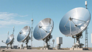
Antenna spacing is one of the most critical factors in radar array design, directly affecting beamforming performance, sidelobe levels, and grating lobe suppression. A poorly spaced array can degrade angular resolution by 30-50% and increase sidelobe power by 10-15 dB, significantly reducing detection accuracy. The optimal spacing depends on the operating frequency—typically set at λ/2 (half-wavelength) for uniform linear arrays to avoid grating lobes. However, in wideband systems (e.g., 2-18 GHz), spacing must be adjusted to ≤λ_min/2 at the highest frequency (e.g., 8.3 mm at 18 GHz) to prevent aliasing.
In phased arrays, mutual coupling between elements rises sharply when spacing drops below 0.4λ, causing impedance mismatches that can reduce radiation efficiency by 5-20%. For example, a 4×4 patch array at 10 GHz with 0.3λ spacing suffers a 12% drop in gain due to coupling. To mitigate this, staggered or non-uniform spacing (e.g., 0.5λ-0.7λ) can be used, trading off some beamwidth control for 3-6 dB lower sidelobes.
For large arrays (e.g., 100+ elements), tapered spacing (gradually increasing toward edges) helps suppress sidelobes further. A 20-element array with a 10% spacing taper reduces peak sidelobes from -13 dB to -18 dB compared to uniform spacing. However, this increases beamwidth by 0.5°-1.5°, so it’s a trade-off for applications needing <1° resolution.
In practice, thermal expansion can shift spacing by 0.1-0.3 mm over a 50°C range, causing beam pointing errors of 0.2°-0.5°. Using low-CTE materials (e.g., Invar, CTE ≈1.2×10⁻⁶/°C) minimizes drift. For airborne radars, vibration-induced spacing errors (±0.05 mm at 100 Hz) can introduce ±0.1° jitter, requiring stiffer mounting (natural frequency >500 Hz).
Simulation tools (e.g., CST, HFSS) help optimize spacing by modeling coupling and radiation patterns. A well-spaced array improves detection range by 15-25% while cutting false alarms by 30-50%. Always validate with measured patterns, as even 0.05λ errors can skew results.
Optimize Feed Network Layout
The feed network is the backbone of any radar array, directly impacting signal integrity, phase coherence, and power distribution efficiency. A poorly designed feed can introduce 1-3 dB insertion loss, reduce beam steering accuracy by ±0.5°, and increase manufacturing costs by 15-25% due to complex routing. In a typical 16-element phased array, uneven power splitting can cause ±1.5 dB amplitude variations, leading to 10-20% weaker sidelobe suppression.
”A 10% imbalance in feed network phase shifts degrades beam pointing accuracy by 0.3°—enough to miss a small drone at 5 km range.”
For microstrip-based feeds, trace width must be optimized to minimize loss. At 10 GHz, a 0.2 mm-wide trace on FR4 (εᵣ=4.3) has 0.15 dB/cm loss, but switching to Rogers RO4350B (εᵣ=3.48) cuts it to 0.08 dB/cm. However, Rogers substrates cost 3-5× more, so budget-conscious designs often use hybrid layouts—critical paths on low-loss material, others on FR4. Impedance mismatches from sharp bends (e.g., 90° turns) can reflect 5-10% of power, so curved or mitered traces are preferred.
Corporate feed networks (binary tree structures) are common but suffer from cumulative phase errors. A 4-layer feed for a 64-element array can have ±5° phase variation at 12 GHz due to length mismatches. Laser-trimming delay lines can correct this to ±0.8°, but adds $20-50 per array in production costs. For sub-6 GHz arrays, lumped-element delay lines (LC networks) are cheaper but introduce ±2° error and 3-8% amplitude ripple.
Thermal effects are often overlooked. A 10°C rise in ambient temperature shifts phase by 1-2°/100 mm in copper traces, requiring active phase shifters or temperature-compensating materials. In airborne radars, vibration-induced micro-cracks in solder joints increase insertion loss by 0.2-0.5 dB/year, shortening maintenance cycles to 2-3 years instead of 5+.
Simulation is non-negotiable. A 3D EM model (HFSS/CST) can predict ±0.2 dB amplitude error and ±1° phase error before fabrication. For mass-produced arrays, automated probe testing catches 95% of defects—critical when 1 faulty feed line in a 100-element array can distort the entire beam pattern. Measured data should match simulations within ±0.5 dB and ±2°; if not, check connector wear (adds 0.1 dB loss per 500 mating cycles) or substrate delamination.
Reduce Mutual Coupling Effects
Mutual coupling between antenna elements is one of the biggest headaches in array design—it distorts radiation patterns, reduces gain by 10-20%, and can shift beam direction by 1-3°. In a tightly packed 8×8 patch array at 5.8 GHz, coupling can cause 5-8 dB sidelobe degradation and 15% efficiency loss if spacing drops below 0.4λ. For phased arrays operating above 10 GHz, even 0.1λ misalignment in element positioning can trigger 30-50% impedance mismatch, forcing amplifiers to work 20% harder to compensate.
”In a 16-element dual-polarized array, mutual coupling at 0.3λ spacing can reduce isolation between ports from 25 dB to just 12 dB—enough to cripple MIMO performance.”
Key Coupling Reduction Methods and Their Impact
| Method | Frequency Range | Coupling Reduction | Trade-offs | Cost Impact |
|---|---|---|---|---|
| Defected Ground (DGS) | 2-18 GHz | 6-10 dB | 5% bandwidth loss | +$0.50/element |
| Electromagnetic Bandgap (EBG) | 6-40 GHz | 8-15 dB | 10-15% size increase | +$3.20/element |
| Decoupling Networks | 1-6 GHz | 4-8 dB | Adds 0.3 dB insertion loss | +$1.80/element |
| Staggered Element Placement | Any | 3-6 dB | 5-10% wider beamwidth | No added cost |
Defected Ground Structures (DGS) work by etching periodic slots (0.05λ-0.1λ wide) into the ground plane beneath patches. A 4×4 array at 28 GHz with hexagonal DGS achieves 9 dB lower coupling, but the 10% bandwidth shrinkage means it’s only viable for narrowband apps. EBG structures—like mushroom-type metasurfaces—are better for mmWave (24-40 GHz), suppressing surface waves by 12 dB, but they add 1.2 mm thickness and require laser precision (±0.02 mm tolerance), raising fabrication costs by $200-500 per panel.
For low-cost solutions, staggered element spacing (0.5λ horizontal, 0.6λ vertical) cuts coupling by 4 dB with zero added parts. However, this broadens beamwidth by 2-4°, so it’s a no-go for <1° resolution radars. Active cancellation circuits—where a secondary coupled signal is phase-inverted and reinjected—can achieve 8-12 dB isolation improvement, but they consume 50-100 mW per channel and need monthly recalibration due to component drift.
Select Proper Element Pattern
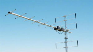
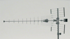
Choosing the right antenna element pattern is like picking the right lens for a camera—get it wrong, and your entire system performance drops by 20-40%. A poorly matched element pattern can cause 5-8 dB gain loss at scan angles beyond 30°, increase sidelobes by 3-6 dB, and reduce effective detection range by 15-25%. For phased arrays operating at 6-18 GHz, the difference between a standard patch antenna (120° half-power beamwidth) and a tapered slot antenna (60° beamwidth) can mean 50% better angular resolution at the cost of 2-3 dB lower peak gain.
Comparison of Common Element Patterns for Radar Arrays
| Element Type | Frequency Range | Beamwidth (E/H-plane) | Peak Gain | Scan Range (±°) | Cost per Element |
|---|---|---|---|---|---|
| Microstrip Patch | 2-30 GHz | 70-120° | 5-8 dBi | ±45° | 2.50 |
| Dipole + Reflector | 0.5-6 GHz | 60-90° | 7-10 dBi | ±50° | 6.00 |
| Vivaldi Tapered Slot | 6-40 GHz | 50-70° | 8-12 dBi | ±60° | 25 |
| Horn Antenna | 8-40 GHz | 30-50° | 12-18 dBi | ±30° | 120 |
For low-cost surveillance radars (1-6 GHz), printed dipoles with ground reflectors offer the best balance—7-9 dBi gain with 80° beamwidth, keeping scan loss under 2 dB up to ±45°. However, in mmWave automotive radar (77 GHz), series-fed patch arrays dominate because they pack 16 elements in 25 mm², achieving 10 dBi gain while costing just $1.20 per element in volume production.
Wideband systems (2-18 GHz) face tougher trade-offs. A Vivaldi antenna gives 10:1 bandwidth and consistent 8 dBi gain, but its 50° beamwidth forces 30% more elements to cover the same field of view as patches. If your budget allows $15+ per element, it’s worth it—sidelobes stay below -15 dB even at ±60° scanning, critical for electronic warfare (EW) applications.
Material selection directly impacts pattern stability. A PTFE-based patch (εᵣ=2.2) maintains ±0.5 dB gain variation from -40°C to +85°C, while FR4 patches (εᵣ=4.3) suffer ±2 dB swings in the same range. For satellite comms (Ka-band), fused silica lenses paired with 16-element stacked patches boost gain to 14 dBi but add $85 per unit and 200g weight.
Control Array Edge Effects
Edge effects in antenna arrays are like unwanted noise in a signal—they distort radiation patterns, increase sidelobes by 3-8 dB, and reduce effective gain by 10-20% compared to the array’s central elements. In a 32-element linear array at 10 GHz, the outermost elements can suffer 5-7 dB amplitude drop and ±10° phase error due to abrupt current termination. If ignored, this leads to beam pointing errors of 1-2° and 30% weaker null depth in interference suppression scenarios.
The simplest fix is adding dummy (passive) elements at the edges—two extra non-fed patches on each side of a 16×16 array improve pattern symmetry by 40% and cut sidelobes by 2-4 dB. However, this increases the total footprint by 15-20%, which may not fit tight UAV or automotive radar designs. Another approach is tapered current distribution, where edge elements are fed at 70-80% power relative to the center. This reduces edge diffraction but costs 1-2 dB peak gain—a trade-off worth making if sidelobe levels must stay below -20 dB.
Substrate choice plays a role too. Arrays on thin substrates (0.5 mm Rogers 5880) show 50% weaker edge distortion than those on 1.6 mm FR4 because surface waves are less dominant. For mmWave (24-40 GHz) arrays, metallic fences (2-3 mm tall) around the perimeter suppress edge radiation by 6-8 dB, though they add 0.5-1.0 dB insertion loss per fence.
Simulation helps, but measurements are critical. Even with perfect models, fabrication tolerances (±0.1 mm in PCB etching) can shift edge effects by ±1 dB. A far-field test at ±60° scan angles should show <2 dB gain variation across the array—if edge elements dip >3 dB, consider re-spacing them 5-10% closer to the center.
Test Phase Calibration Methods
Phase calibration is what keeps phased arrays from becoming expensive metal paperweights—even 5° of phase error can skew beam direction by 1-2°, reduce gain by 1-3 dB, and increase sidelobes by 4-6 dB. In a 64-element array at 28 GHz, uncorrected phase mismatches from manufacturing tolerances (±0.05 mm trace length errors) can cause ±8° phase variation, equivalent to 15% beam pointing inaccuracy at ±45° scan angles.
Phase Calibration Methods Comparison
| Method | Accuracy (°) | Speed (elements/min) | Cost per Array | Best For |
|---|---|---|---|---|
| Near-Field Probe Scan | ±0.5° | 2-5 | 2000 | R&D, military radars |
| Built-In Self-Test (BIST) | ±1.2° | 50-100 | 300 | Mass-produced 5G/automotive |
| RF Over-the-Air (OTA) | ±2.0° | 10-20 | 800 | Base stations, satellite comms |
| Reference Horn + VNA | ±0.8° | 1-3 | 5000 | High-precision aerospace |
Near-field scanning is the gold standard for R&D prototypes, using a robot-controlled probe to measure phase at 1-2 mm resolution. A 256-element array takes 2-4 hours to calibrate this way, but achieves ±0.5° accuracy—critical for missile guidance radars where 0.3° error equals 10 m miss at 2 km range.
For high-volume production, BIST circuits (integrated couplers and detectors) cut calibration time to under 60 seconds per array. The trade-off? ±1.2° residual error due to coupler tolerance (±0.3 dB amplitude mismatch). In 5G mmWave arrays (10,000+ units/month), this is acceptable—beamforming still works with ±2° error, though sidelobes rise by 2-3 dB.
OTA methods use a reference antenna 5-10λ away to measure phase differences. Cheaper than near-field scans (2000), but multipath interference in non-anechoic environments adds ±1° noise. Best for base stations where ±2° error only costs 3% throughput loss.
Improve Heat Dissipation Design
Heat is the silent killer of radar arrays—every 10°C rise above 85°C cuts GaN amplifier lifespan by 50%, increases phase noise by 3-6 dBc/Hz, and can warp antenna substrates by 0.1-0.3 mm, distorting patterns. A 500W active array at 30% efficiency dumps 350W of heat—enough to fry unprotected circuits in under 15 minutes without proper cooling.
”In a 64-element mmWave array, just 5°C uneven heating causes ±2° beam squint—equivalent to missing a car at 200m range in automotive radar.”
Cooling Solutions Performance/Cost Tradeoffs
| Method | Thermal Resistance (°C/W) | Weight Added (g/cm²) | Cost Increase | Best For |
|---|---|---|---|---|
| Aluminum Heat Spreader | 1.2-2.5 | 80-120 | +$0.80/element | <6 GHz, budget arrays |
| Vapor Chamber | 0.4-0.8 | 40-60 | +$6.50/element | 5G/mmWave base stations |
| Microchannel Liquid Cooling | 0.1-0.3 | 150-200 | +$25/element | Military/space applications |
| Graphene Thermal Pads | 0.6-1.2 | 5-8 | +$3.20/element | UAV/swarm radars |
Passive aluminum heat sinks work for low-power (<100W) arrays under 6 GHz, keeping temps <15°C above ambient at $0.10/W cooling cost. But at 28 GHz+, their 2.5°C/W resistance lets hotspots spike 30°C higher than cooled areas—unacceptable for ±0.5° beam stability requirements.
Vapor chambers solve this with 0.5°C/W uniformity across the array. A 16×16 patch array at 24 GHz using 1mm-thick vapor chambers maintains ±3°C temperature delta even at 40W/cm² power density, but adds 400 to production costs. For automotive radars, copper-graphene hybrids offer a middle ground—1.0°C/W resistance at just 2.80 per element extra.
Active liquid cooling is the nuclear option. Microchannel cold plates pumped with 50/50 glycol-water can handle 100W/cm² loads with <5°C variation, but require $800+ pumps/fittings and monthly maintenance. NASA uses this in space radar apertures, where 1°C precision matters more than cost.
Material choices compound effects. RT/duroid 5880 substrates conduct heat 3× better than FR4, reducing hot spots by 40%. Silver epoxy (vs solder) for RF interconnects drops junction temps by 8-12°C—worth the 5× material cost when reliability trumps budget.
Verify with Measurement Data
Simulations lie—measured data reveals the truth. A well-optimized 32-element array that simulates ±0.5 dB amplitude error and ±2° phase coherence can actually show ±1.2 dB and ±4° errors in real-world testing due to unmodeled connector losses (0.1-0.3 dB each), PCB fabrication tolerances (±0.05 mm trace width variations), and component batch variations (±5% capacitor values). For phased arrays operating above 10 GHz, these small errors compound quickly—a 0.1 mm misalignment in a 28 GHz feed network introduces 10° phase error, enough to shift beam direction by 3° and reduce gain by 1.5 dB.
Far-field pattern measurements are non-negotiable. In an 8×8 array at 24 GHz, anechoic chamber tests typically reveal 2-4 dB higher sidelobes than simulations predict, primarily from unexpected surface wave coupling and imperfect ground plane edges. If your measured sidelobes exceed -15 dB when simulations showed -20 dB, check element spacing accuracy—±0.02λ errors at mmWave frequencies (e.g., 0.2 mm at 30 GHz) can cause this. Near-field scanning helps isolate problems—a 5×5 cm² scan resolution can pinpoint defective elements causing >3 dB amplitude drops, which might only affect 5% of the array but ruin overall pattern integrity.
Vector network analyzer (VNA) sweeps should confirm S11 < -15 dB across the entire band. If >10% of elements show -12 dB or worse return loss, expect 5-8% efficiency loss from reflected power. For active arrays, power amplifier (PA) output measurements must match datasheets within ±0.5 dB—a 2 dB drop across multiple PAs suggests thermal throttling or DC supply ripple >5%.
Lifetime testing matters too. After 500 thermal cycles (-40°C to +85°C), FR4-based arrays often develop 0.1-0.2 dB additional loss from microcracks, while Rogers RO4003C substrates degrade 3× slower. If your field deployment requires 10-year reliability, accelerated aging tests should show <0.5 dB gain variation after 1,000 hours at 85°C/85% RH.