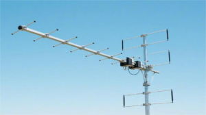
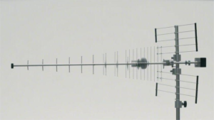
To test waveguide components for signal loss, use a vector network analyzer (VNA) to measure insertion loss by comparing the transmitted signal power through the component to a known reference, typically aiming for losses below 0.1 dB in high-performance systems. Ensure proper flange alignment and calibration with thru-reflect-line (TRL) kits for millimeter-wave accuracy.
Table of Contents
Understanding Signal Loss Basics
For instance, a high-quality waveguide bend might only introduce 0.1 dB of loss, meaning over 98% of the input power successfully passes through. Conversely, a poorly manufactured joint can cause losses exceeding 1.0 dB, dissipating more than 20% of the signal power as heat and drastically reducing system range and efficiency. Understanding these metrics is the first step to accurate measurement.
| Loss (dB) | Percentage of Power Transmitted | Typical Component Example |
|---|---|---|
| 0.1 dB | 97.7% | High-quality straight section |
| 0.5 dB | 89.1% | A well-mated flange connection |
| 1.0 dB | 79.4% | A simple horn antenna or a long corrugated cable |
| 3.0 dB | 50.0% | A significant obstacle, like a damaged waveguide |
The primary contributor is Ohmic (or conductor) loss, caused by the electrical resistance of the waveguide’s metal walls. At 10 GHz, the skin depth in copper is only about 0.66 micrometers, forcing current to flow in a thin layer and generating heat. The loss is directly proportional to the square root of frequency; doubling the frequency increases loss by approximately 1.414 times. This means a 40 GHz system has inherently higher baseline loss than a 15 GHz one.
Dielectric loss, though often smaller, occurs from energy absorption within any insulating material inside the guide, like a pressurized gas or supporting dielectric rods. For dry air, this loss is negligible, often less than 0.001 dB/meter.
Setting Up Measurement Equipment
For most waveguide bands, a 2-port model with a frequency range exceeding your test band by at least 5% is essential. Before any measurement, the VNA must be calibrated to establish a known reference plane, typically reducing measurement uncertainty to less than ±0.05 dB. Using a high-quality calibration kit specific to your waveguide size (e.g., WR-90 for 8.2-12.4 GHz) is non-negotiable for trustworthy data.
| Equipment | Key Specification | Impact on Accuracy |
|---|---|---|
| Vector Network Analyzer (VNA) | ±0.05 dB measurement uncertainty | Directly defines result precision |
| Test Cable & Adapters | Phase stability ±5°, < 0.1 dB loss | Major source of error if low-quality |
| Calibration Kit | ±1 μm mechanical tolerance of standards | Defines the baseline accuracy of the entire setup |
| Frequency Range | Must exceed test band by 5-10% | Ensures reliable data at band edges |
A flexible test cable rated for > 100,000 bend cycles maintains stability. Each adapter between the coaxial cable and waveguide flange introduces a potential 0.02 to 0.1 dB error. Minimize the number of connections. A single, well-made transition is always better than two adapters chained together.
A full 2-port SOLT (Short-Open-Load-Thru) calibration compensates for the system’s imperfections. The physical dimensions of the calibration standards must be precise; a short circuit’s position must be accurate within ±2 microns to ensure a phase accuracy of ±1° at 40 GHz. After calibration, perform a validation check by connecting the calibration standards again. The measured response should be within ±0.02 dB and ±1° of their ideal values. Any deviation beyond this, like a 0.05 dB ripple, indicates a poor connection or damaged standard and requires re-calibration.
Cable movement after calibration can induce > 0.1 dB error. Secure all cables to avoid flexing. Temperature fluctuations of more than ±2°C can cause ±0.02 dB drift in the measurement due to thermal expansion/contraction of the fixtures. Allow the VNA and test setup to stabilize for at least 30 minutes in a 23°C ±3°C lab environment for the most stable readings. The IF bandwidth on the VNA should be set between 100 Hz and 1 kHz as a balance between measurement speed and noise; a lower bandwidth reduces noise but increases sweep time.
Preparing Waveguide for Testing
A single fingerprint smudge on a flange can easily introduce 0.1 to 0.3 dB of loss at 30 GHz. Similarly, a microscopic dust particle trapped between connections can scatter energy, leading to unpredictable and erroneous readings, often varying by ±0.05 dB between measurements. A meticulous, repeatable preparation process is essential for data integrity.
- Visual Inspection: Examine flanges for nicks, scratches, or deformation. A dent deeper than 0.05 mm can compromise the seal.
- Cleaning: Use ≥99% isopropyl alcohol and lint-free swabs to remove all contaminants from mating surfaces.
- Drying: Allow a minimum of 60 seconds for the alcohol to fully evaporate to prevent a dielectric film.
- Connector Torque: Use a torque wrench to tighten flange bolts to the manufacturer’s specification, typically 15-20 inch-pounds (1.7-2.3 Nm).
Begin with a thorough visual inspection under a bright light. Use a 10x magnification loupe to examine the critical mating surface of each flange. Look for scratches, pits, or burrs. A scratch that is 5 μm deep and 2 mm long can act as a slot antenna, radiating energy and causing > 0.1 dB loss. Any flange with a dent exceeding 0.1 mm in depth or visible corrosion should be rejected or professionally refinished, as it will never form a reliable connection.
Cleaning is a non-negotiable step. Even < 1 μg of oil or dust degrades performance. Fold a lint-free swab, moisten it with ≥99% isopropyl alcohol (avoid lower purity as it leaves residues), and vigorously scrub the entire flange surface in a circular motion. Immediately dry the surface with a second, dry lint-free swab. This two-swab method prevents re-depositing contaminants. For persistent contamination, use a swab lightly dampened with high-purity acetone, but be aware it can damage some plastic components and evaporates in < 15 seconds.
Conducting the Loss Measurement
Even with a perfect setup, environmental factors like temperature drift of 0.05°C/minute can cause a measurement drift of ±0.01 dB. Setting the correct VNA parameters and employing averaging are essential to mitigate noise and obtain a reliable insertion loss value, typically aiming for a measurement uncertainty of less than ±0.03 dB.
- Parameter Setup: Configure frequency range, number of points, and IF bandwidth.
- Stabilization: Allow the DUT and cables to settle for > 120 seconds after handling.
- Averaging: Apply 16 to 64 averages to reduce random noise.
- Data Recording: Save both the trace data and a screenshot of the measurement conditions.
Key Principle: Always conduct a ”before and after” reference measurement. First, measure the loss through the test setup withoutthe Device Under Test (DUT)—this is your reference trace (S21_ref). Then, insert the DUT and measure again (S21_dut). The actual DUT loss is the difference: Insertion Loss = S21_ref – S21_dut. This method automatically subtracts the inherent loss of your test fixtures and cables.
Begin by configuring the VNA. Set the start and stop frequencies to match your waveguide’s operational band, for example, 8.0 to 12.5 GHz for WR-90. Use a high number of points, typically 2001, to ensure you have enough data resolution to identify narrow, resonant dips which might indicate a faulty component. Set the IF bandwidth to 100 Hz. This reduces the noise floor by filtering the received signal, but increases the sweep time to approximately 2 seconds per sweep.
Once configured, do not immediately measure. After connecting the DUT, wait for at least 2 minutes. This allows thermal equilibrium to be reached, minimizing drift caused by heat from your hands or the ambient environment. Engage the VNA’s averaging function. Setting it to 64 averages will reduce random noise by a factor of √64, or 8 times, dramatically smoothing the trace. The trade-off is a longer measurement time; 64 averages will take roughly 2 minutes.
Analyzing Measurement Results
For instance, a smooth trace with a 0.5 dB peak-to-peak variation across 10 GHz is normal for a long, corrugated cable, while the same variation over 100 MHz indicates a serious problem. Proper analysis separates random measurement noise (e.g., ±0.02 dB) from systematic component defects.
| Trace Characteristic | Acceptable Range | Indicates a Problem If… |
|---|---|---|
| Overall Smoothness | Gentle, continuous slope | Contains sharp dips/spikes > 0.1 dB over < 50 MHz |
| Noise Floor | < ±0.03 dB ripple with averaging | Ripple exceeds ±0.05 dB after 64 averages |
| Repeatability | < ±0.02 dB difference between runs | Difference between connections is > 0.05 dB |
| Trace Slope | Linear or parabolic change with frequency | Slope is erratic or has discontinuities |
Rule of Thumb: The standard deviation of your trace noise, measured over a 10 MHz span where the signal should be flat, should be less than 0.01 dB. A higher value indicates poor calibration, a faulty connection, or excessive system noise that must be resolved before trusting the results.
First, assess the baseline noise and stability. Zoom in on a 50 MHz section of the trace and measure the peak-to-peak variation. With 64 averages applied, this value should be below 0.05 dB. A value between 0.05 dB and 0.1 dB suggests marginal stability, often due to a slightly imperfect connection or temperature drift. Anything above 0.1 dB means your measurement is unreliable and the setup must be investigated. This noise floor defines the minimum loss you can confidently resolve.
Next, analyze the shape of the loss curve. A healthy component exhibits a relatively smooth, predictable response. Calculate the average loss across the entire band, but pay more attention to the maximum loss value and its location. A peak loss of 0.8 dB at 24.5 GHz is a more critical design constraint than an average loss of 0.5 dB. Use the VNA’s marker search functions to find these global maximum and minimum points precisely. Also, calculate the total ripple: (Max Loss – Min Loss). A ripple value exceeding 0.7 dB for a simple straight waveguide section often indicates internal contamination or surface damage.
Troubleshooting Common Issues
A high noise floor of ±0.08 dB or a loss value that changes by 0.15 dB between successive measurements are clear red flags. These problems often stem from a small set of common, fixable causes. A systematic approach to troubleshooting, starting with the most probable culprit, can save hours of diagnostic time and prevent the reporting of erroneous data.
The most frequent issue is high measurement noise and instability, characterized by a trace that flickers or shifts by more than ±0.03 dB. This is almost always caused by a problem in the connections. First, check that all connectors are torqued to the correct specification, typically 18 ±2 inch-pounds. A loose connection, even one under-torqued by just 5 inch-pounds, can act as a tiny antenna, injecting noise. Second, inspect for microscopic contamination. Residue from a single fingerprint can increase loss by 0.1 to 0.3 dB and cause noise. Rec clean all flange faces with ≥99% isopropyl alcohol and lint-free swabs, ensuring a minimum 60-second drying time. Third, check for mechanical movement. Any vibration or movement in the test cables after calibration will destroy measurement integrity. Secure all cables so that the last 30 cm before the DUT is completely stationary.
If the noise is low but the measured loss is unexpectedly high, the problem may be calibration or the DUT itself. First, verify your calibration by re-measuring the Short and Load standards. The return loss for the Load standard should be better than 35 dB and the Short should show a consistent 180-degree phase shift across the band. A deviation of more than 3 degrees at a band edge indicates a faulty or dirty standard. Second, perform a simple time-domain reflectometry (TDR) measurement if your VNA supports it. A TDR plot can reveal the precise location of an imperfection. A spike in the TDR response 15 cm into the DUT indicates an internal obstruction or dent at that exact point, which might be causing a 0.4 dB loss.
When results are inconsistent between connections (repeatability standard deviation σ > 0.04 dB), the cause is typically mechanical wear or damage. Examine the flange mating surfaces under 10x magnification. Look for polishing marks that are no longer uniform, which indicates wear. A wear depth of just 5 micrometers can be enough to cause a 0.05 dB variation between connections.