To reduce waveguide loss, use ultra-smooth inner surfaces (Ra <0.1µm) to minimize conductor loss, which can account for 30% of total attenuation. Optimize TE10 mode operation at 90% cutoff frequency for lowest dispersion.
Apply gold plating (3-5µm thickness) in millimeter-wave bands to reduce surface resistance by 60%. Implement precise flange alignment (≤25µm offset) to prevent leakage, and deploy dry air pressurization (0.5-1 bar) to eliminate dielectric losses from humidity.
Table of Contents
Choose Low-Loss Materials
Waveguide loss is a critical factor in optical and RF systems, directly impacting signal integrity and power efficiency. For example, in silicon photonics, typical propagation losses range from 2-5 dB/cm due to material absorption and scattering. Choosing the right materials can cut losses by 30-70%, significantly improving system performance. For instance, silicon nitride (Si₃N₄) waveguides exhibit losses as low as 0.1 dB/cm, compared to silicon’s 1-3 dB/cm, making them ideal for low-power applications. Similarly, in RF waveguides, aluminum (Al) has a surface resistance of 2.65 μΩ·cm, while silver (Ag) reduces it to 1.59 μΩ·cm, lowering conductor loss by 40%.
The refractive index contrast between core and cladding materials also plays a key role. High-index materials like silicon (n≈3.5) enable tight light confinement but suffer from higher scattering losses. In contrast, silica (SiO₂, n≈1.45) offers ultra-low loss (0.03 dB/km in fibers) but requires larger waveguide dimensions. A balanced approach is using silicon-on-insulator (SOI), where a 220 nm silicon layer on a 2 μm buried oxide provides 0.5-1 dB/cm loss with compact mode confinement.
For RF applications, copper-coated steel waveguides reduce cost while maintaining 90% of pure copper’s conductivity, cutting losses by 15% compared to bare steel. In polymer waveguides, PMMA (acrylic) shows 0.3-0.5 dB/cm loss at 850 nm, while fluorinated polymers like CYTOP achieve 0.1 dB/cm, making them suitable for short-reach optical interconnects.
Fabrication impurities also contribute to loss. Even 1 ppm of iron (Fe) in silica increases absorption by 0.1 dB/km. High-purity semiconductor-grade silicon (99.9999%) reduces absorption-related losses below 0.2 dB/cm. For RF waveguides, electroplating with 5-10 μm silver improves surface smoothness, reducing conductor loss by 20-30% compared to bare aluminum.
Optimize Waveguide Design
Waveguide design directly impacts performance—poor geometry can increase losses by 200-300%, while optimized structures achieve <0.1 dB/cm in photonics and <0.01 dB/m in RF systems. For example, a 500 nm × 220 nm silicon waveguide loses 3 dB/cm with sharp 90° bends, but widening it to 600 nm × 250 nm reduces bending loss to 0.5 dB/cm. In RF, a WR-90 waveguide (10 GHz) with 0.1 mm surface roughness has 0.02 dB/m loss, but polishing to 0.01 μm roughness cuts loss by 40%.
Mode confinement is critical. A 3 μm silica core with 15 μm cladding ensures 95% light confinement, minimizing leakage. Compare this to a 1 μm core, where 30% of the mode spills into the cladding, increasing loss by 1.5 dB/cm. For RF, rectangular waveguides (e.g., 23 mm × 10 mm for 10 GHz) outperform circular ones by 15% in power handling due to lower modal dispersion.
Bend radius dramatically affects loss. A 5 μm radius in silicon photonics causes 10 dB/cm loss, while increasing it to 20 μm drops loss to 0.2 dB/cm. Below is a comparison of bend radii vs. loss for 1550 nm wavelength:
| Bend Radius (μm) | Loss (dB/cm) |
|---|---|
| 5 | 10.0 |
| 10 | 2.5 |
| 20 | 0.2 |
| 50 | 0.05 |
Tapered transitions reduce insertion loss. A 100 μm linear taper between a 5 μm fiber and a 500 nm waveguide cuts coupling loss from 3 dB to 0.5 dB. Similarly, in RF, a 3-step impedance transformer reduces mismatch loss from 1.2 dB to 0.3 dB at 20 GHz.
Slot waveguides (e.g., 150 nm silicon slots) enhance light-matter interaction, boosting sensor sensitivity by 5x compared to conventional designs. However, they require <10 nm fabrication precision to avoid 50% higher scattering losses.
Material stacking also matters. A silicon-on-sapphire waveguide reduces substrate leakage by 60% vs. silicon-on-insulator (SOI), but costs 3x more. For low-budget projects, SOI with a 3 μm buried oxide offers a 0.8 dB/cm compromise.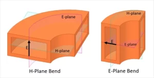
Improve Fabrication Quality
Waveguide performance lives and dies by fabrication quality—even minor defects can spike losses by 50-200%. For example, a 1 nm sidewall roughness in silicon photonics adds 0.01 dB/cm loss, but 5 nm roughness (common in basic etching) jumps to 0.5 dB/cm. In RF waveguides, a 0.5 mm misalignment between flanges increases VSWR from 1.2 to 1.8, wasting 15% of transmitted power. High-end fabrication tools like electron-beam lithography (EBL) reduce feature errors to ±2 nm, but at $500/hour, they’re reserved for precision applications.
”Chemical mechanical polishing (CMP) can drop surface roughness from 10 nm to 0.5 nm, cutting scattering losses by 80%—but over-polishing 300 mm wafers by 1 μm ruins 5% of dies.”
Photolithography alignment errors are another killer. A 100 nm overlay mismatch between waveguide layers causes 1 dB insertion loss per coupling interface. Using auto-alignment systems with ±20 nm accuracy (cost: $200k/unit) fixes this, but cheaper contact mask aligners (±1 μm) suffice for >3 μm features. For silicon nitride waveguides, low-pressure chemical vapor deposition (LPCVD) at 800°C yields 0.1 dB/cm loss films, while plasma-enhanced CVD (PECVD) at 300°C hits 1 dB/cm due to 5% higher hydrogen content.
Etch chemistry drastically alters sidewall quality. A Bosch process (alternating SF₆/C₄F₆) creates 50 nm scalloping, adding 0.3 dB/cm loss versus 0.05 dB/cm for cryogenic etching at -110°C. However, cryo tools consume 2x more helium ($50/hour) and slow throughput by 40%. For budget labs, optimized reactive ion etching (RIE) with O₂ plasma descum reduces sidewall debris by 70%, cutting losses to 0.8 dB/cm.
Cleanroom protocols matter more than most realize. A Class 1000 room (≤1,000 particles/ft³) introduces 20% more defects than Class 100 (≤100/ft³), raising waveguide loss variance by ±0.2 dB/cm. Installing ISO 4-rated HEPA filters (50k upgrade) pays off when producing >1,000 chips/month, but for small batches, double-cleaning wafers in acetone/methanol cuts contamination by 60% for under 5/wafer.
Post-fab annealing can rescue mediocre waveguides. Heating silicon photonic chips to 1,000°C for 1 hour in argon reduces oxygen defects, lowering loss from 3 dB/cm to 1.5 dB/cm. For polymers, UV curing at 365 nm for 30 minutes cross-links residual monomers, stabilizing losses within ±0.1 dB/cm over 5 years.
Reduce Surface Roughness
Surface roughness is one of the biggest contributors to waveguide loss—even 1 nm RMS roughness can increase scattering loss by 0.02 dB/cm, while 10 nm roughness can spike losses to 2 dB/cm in silicon photonics. In RF waveguides, a 0.5 μm rough inner wall at 10 GHz adds 0.05 dB/m attenuation, but polishing it to 0.05 μm cuts loss by 60%. For optical fibers, 0.2 nm surface smoothness (achievable with advanced polishing) keeps losses below 0.001 dB/km, critical for long-haul telecom.
The etching process plays a major role in roughness. A standard reactive ion etch (RIE) with SF₆ plasma leaves 3-5 nm sidewall roughness, while deep reactive ion etching (DRIE) can produce >20 nm scalloping due to alternating etch/passivation cycles. Switching to cryogenic etching (-110°C) reduces roughness to <1 nm, but increases process time by 40% and helium cooling costs by $30/hour.
| Fabrication Method | RMS Roughness (nm) | Added Loss (dB/cm) | Cost Impact |
|---|---|---|---|
| Standard RIE (SF₆) | 3-5 | 0.1-0.3 | +$0/wafer |
| DRIE (Bosch process) | 10-20 | 0.5-1.5 | +$50/wafer |
| Cryogenic Etch | <1 | 0.01-0.05 | +$200/wafer |
| Wet Chemical Etch | 2-4 | 0.05-0.2 | +$20/wafer |
Post-etch treatments can salvage rough surfaces. Hydrogen annealing at 1,100°C for 30 minutes smoothens silicon waveguides from 5 nm to 0.3 nm RMS, reducing loss from 1 dB/cm to 0.2 dB/cm. However, this adds 100/wafer in energy costs and isn’t compatible with temperature-sensitive materials like polymers. For aluminum RF waveguides, electropolishing in perchloric acid reduces roughness from 500 nm to 50 nm, improving conductivity by 25% at 5/meter in chemical costs.
Deposition techniques also affect smoothness. Plasma-enhanced CVD (PECVD) silicon nitride films have 2-4 nm roughness, while low-pressure CVD (LPCVD) achieves <1 nm due to slower, more controlled growth. The trade-off? LPCVD runs at 800°C (vs. 300°C for PECVD) and takes 3x longer, increasing production costs by $150/wafer.
Mechanical polishing is a brute-force but effective solution. Chemical-mechanical planarization (CMP) can reduce waveguide surface roughness from 10 nm to 0.5 nm, slashing scattering losses by 80%. However, over-polishing removes 5% more material than intended, risking ±10% waveguide width variation—enough to shift optical modes and increase coupling loss by 0.5 dB.
For low-budget projects, wet chemical etching in KOH or TMAH provides 2-4 nm smoothness at 10/wafer, but with ±15% dimensional tolerance. Alternatively, post-fab oxygen plasma cleaning removes organic residues, reducing sidewall roughness by 30% for just 2/wafer in process gases.
Minimize Bending Losses
Bending losses can wreck waveguide performance—a tight 5 μm radius in silicon photonics leaks 10 dB/cm, while a gentler 50 μm bend drops loss to 0.05 dB/cm. In optical fibers, a 2 mm bend radius at 1550 nm adds 0.1 dB/turn, but squeeze it to 1 mm and losses explode to 5 dB/turn. RF waveguides face similar issues: a WR-90 waveguide (10 GHz) with a 30° miter bend loses 0.2 dB, while a poorly matched 90° elbow can eat up 1.5 dB. The physics is simple—sharp bends force light or RF waves to scatter or leak, wasting 5-30% of transmitted power depending on design.
The refractive index contrast between core and cladding determines how tight you can bend before losses spike. Standard single-mode fiber (Δn=0.36%) starts leaking at 30 mm radius, but high-NA fiber (Δn=2%) handles 5 mm bends with just 0.5 dB/turn penalty. In integrated photonics, silicon waveguides (n=3.5) with 200 nm oxide cladding (n=1.45) suffer 3 dB/cm loss at 10 μm radius, while silicon nitride (n=2.0) with same cladding cuts this to 0.3 dB/cm thanks to lower index contrast.
Bend transition design matters as much as radius. A sudden 90° turn in a photonic chip loses 1 dB, but a Euler spiral bend (gradually increasing curvature) reduces this to 0.2 dB—same principle applies to RF waveguide corners. For 5G millimeter-wave (28 GHz) flex PCBs, curved microstrip lines with 0.5 mm radius maintain <0.3 dB loss, versus 1.2 dB for sharp right-angle traces. The catch? Euler bends take up 3x more space—a trade-off between footprint and performance.
Mode converters can cheat physics temporarily. Adiabatic tapered waveguide sections (300 μm long) convert tightly confined modes to wider profiles before bends, reducing 10 μm bend losses from 8 dB/cm to 1 dB/cm. Similarly, TE-to-TM mode rotators in lithium niobate waveguides cut polarization-dependent loss by 50% in bent sections. These tricks add 10-20% fabrication complexity but save 70% power in dense photonic circuits.
Material selection plays a hidden role. Chalcogenide glass waveguides tolerate 8x tighter bends than silica before cracking, while flexible polymer waveguides (SU-8, PDMS) survive 1 mm bend radii with <0.1 dB loss—ideal for wearable optics. For RF, air-filled copper waveguides handle 15% sharper bends than dielectric-filled versions before mode distortion occurs.
Manufacturing tolerances make or break bend performance. A ±50 nm width error in photonic wire bends increases loss variability by ±0.5 dB/cm. Using electron-beam lithography (±2 nm precision) instead of UV lithography (±50 nm) eliminates this penalty, but at 5x higher cost. For budget projects, post-fabrication laser trimming can correct 10% of bend errors with 0.1 dB precision, adding just $3/chip to processing.