Optimize waveguide transfer switches by using precision-machined components with surface roughness below 0.1 µm, ensuring perfect alignment to minimize insertion loss to under 0.1 dB and VSWR below 1.05 through rigorous vector network analyzer testing.
Table of Contents
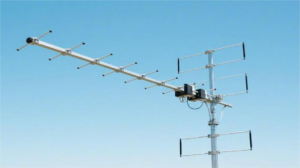
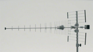
Understanding Waveguide Switch Basics
A typical high-performance switch operating in the 18–40 GHz range might exhibit an insertion loss of just 0.5 dB, meaning over 89% of the signal power is successfully transmitted. In contrast, poorly designed switches can suffer losses exceeding 2 dB, wasting more than 37% of the input power. These losses directly impact system efficiency, especially in applications like satellite communications or radar, where every fractional dB loss can degrade performance over long distances. The physical dimensions of the waveguide also play a key role; for example, a standard WR-42 waveguide (used for Ka-band applications) has an internal cross-section of 10.67 mm × 4.32 mm, and even a 50 µm misalignment in the switch mechanism can increase loss by 0.3 dB or more.
The primary function of a waveguide switch is to route signals between ports with high isolation (often >60 dB) and low voltage standing wave ratio (VSWR, typically <1.20:1). Most commercial switches use electromechanical or solenoid-based actuation, with switching speeds ranging from 10 to 100 milliseconds. The lifetime of these devices is usually specified in cycles; a well-built switch can endure over 1 million cycles with minimal degradation in performance. Materials matter greatly: the inner conductor surfaces are often gold-plated (thickness 0.5–1.5 µm) to reduce resistivity and minimize ohmic losses, which can account for up to 40% of total signal loss in poorly coated designs. The dielectric components, such as support beads, are made from low-loss materials like PTFE (tan δ <0.0005) to avoid unnecessary absorption.
| Parameter | Typical Value | Impact on Loss |
|---|---|---|
| Insertion Loss | < 0.6 dB | Direct power reduction |
| VSWR | < 1.25:1 | Reflection-induced loss |
| Operating Frequency | 18–40 GHz | Design-specific optimization |
| Isolation | > 60 dB | Signal leakage control |
| Actuation Time | 20 ms | System response delay |
| Life Cycles | 1,000,000+ | Long-term reliability |
| Operating Temperature | -40°C to +85°C | Environmental stability |
Waveguide switches are often designed with precision-machined aluminum or brass bodies to ensure dimensional stability under thermal stress. The internal surface roughness should be kept below 0.8 µm RMS to reduce scattering losses. In high-power applications (e.g., 5 kW peak power), corona and multipaction breakdown can become concerns, so pressurization or specialized coatings are used to increase power handling. Proper flange alignment is another practical detail; using UG-style flanges with dowel pins can cut installation-related losses by up to 0.2 dB compared to loose-fit designs.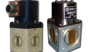
Key Factors Affecting Signal Loss
in a standard Ka-band system operating at 30 GHz, a total loss of just 1.5 dB can result in a 30% drop in output power, significantly reducing link budget margins. These losses primarily stem from impedance mismatches, material properties, mechanical imperfections, and environmental conditions. Understanding each factor quantitatively is essential for engineers who aim to optimize systems where performance margins are tight, such as in 5G backhaul or satellite payloads, where every 0.1 dB loss counts toward overall bit error rate (BER) and system availability.
The surface roughness of the waveguide interior is a major contributor. For instance, an RMS roughness of 1.2 µm can increase conductive loss by approximately 15% compared to a smoother surface with 0.4 µm roughness. This is because RF currents concentrate at the conductor surface (skin effect), and irregularities scatter energy, converting it into heat. In numerical terms, for a copper waveguide operating at 30 GHz, the attenuation constant α increases by nearly 0.01 dB per meter for every 0.5 µm increase in roughness beyond the optimal sub-micron finish.
Impedance discontinuities at junctions or flanges are another critical issue. A misalignment of just 100 µm between two waveguide sections can cause a return loss degradation of 15 dB, effectively increasing VSWR from 1.15 to over 1.35. This mismatch reflects power, and in a high-power system handling 2 kW CW, a 1.5 VSWR can lead to localized heating exceeding 80°C at the flange interface, accelerating oxidation and further increasing loss over time. The use of hard gold plating (1–2 µm thick) on contact surfaces reduces surface resistivity to about 5 mΩ per square, minimizing ohmic losses which can otherwise consume up to 0.4 dB per switch transition.
Dielectric losses in support structures or gas fillings also play a role. While air has a loss tangent (tan δ) of nearly 0, some support beads made from inferior PTFE can have a tan δ of 0.002, adding 0.05 dB per bead at 40 GHz. In switches with multiple internal supports, this can accumulate to 0.2 dB of avoidable loss. Additionally, humidity ingress—especially in non-pressurized systems—can increase effective tan δ. For example, at 85% relative humidity, attenuation can rise by 0.1 dB/m due to water vapor absorption peaks around 22 GHz and 60 GHz.
Thermal effects cannot be ignored. Aluminum waveguides have a thermal expansion coefficient of 23 µm/m°C. A temperature shift from 20°C to 70°C can cause a 1.15 mm length change in a 500 mm long run, potentially misaligning mechanical switches and increasing loss by 0.25 dB if not compensated. Finally, manufacturing tolerances matter: a deviation of just 50 µm in broadwall dimension of a WR-28 waveguide can shift the cutoff frequency by 0.5 GHz, leading to higher modal conversion and loss, especially near band edges.
Material Selection for Low Loss
The inner conductor surface finish can alter conductive losses by over 40% at Ka-band frequencies. A standard aluminum waveguide with a silver plating (4–5 µm thick) might exhibit an insertion loss of 0.4 dB per meter at 40 GHz, while an unplated aluminum surface could see losses exceeding 0.7 dB per meter due to higher surface resistivity and oxidation. In high-volume production, selecting the optimal material combination can reduce total system noise temperature by up to 15 Kelvin in receiver applications, directly improving signal-to-noise ratio (SNR). With switch lifetimes often exceeding 1 million cycles, material wear resistance also becomes critical to maintaining performance over a 10–15 year operational lifespan.
The primary goal is to minimize resistive (ohmic) losses, which dominate at frequencies above 18 GHz. Here’s a breakdown of key material considerations:
- Conductive Coatings: Electrodeposited silver offers the lowest resistivity (~1.6 μΩ·m) but tarnishes over time. Gold plating (0.5–2 µm thick) is more stable in humid environments and provides a surface resistivity of ~4 mΩ/sq, but at a 30% higher cost than silver. For example, a 3-inch-long switch section plated with hard gold adds ~$45 to the unit cost but ensures consistent loss below 0.5 dB even after 500,000 actuations.
- Base Material: Aluminum 6061 is common due to its low density (2.7 g/cm³) and good machinability, but its thermal expansion coefficient (23.6 µm/m°C) can cause dimensional shifts under thermal load. Invar (iron-nickel alloy) has a near-zero expansion coefficient (1.2 µm/m°C) but costs ~5 times more and is 50% heavier. For ground-based systems with stable temperatures, aluminum is sufficient, but aerospace applications often require beryllium-copper (CuBe) springs or housings to maintain contact pressure across a -55°C to +125°C range.
- Dielectric Components: Support beads or radome windows must have minimal loss tangent. PTFE (tan δ ≈ 0.0004) is common, but ceramic-filled composites (e.g., Rogers 4350B, tan δ ≈ 0.0037) offer higher rigidity at the expense of slightly higher loss. For instance, a PTFE support bead introduces ~0.02 dB loss at 30 GHz, while a cheaper nylon bead might add 0.08 dB. In high-power applications (e.g., >3 kW peak), dielectrics must also resist multipaction breakdown, requiring materials with low outgassing rates and high volume resistivity (>10¹⁵ Ω·cm).
- Contact Surfaces: Switching mechanisms rely on spring-loaded contacts, where material choice dictates longevity and contact resistance. Phosphor bronze springs (yield strength ~550 MPa) are cost-effective but may relax after 500,000 cycles. Beryllium copper springs (yield strength ~1100 MPa) maintain force for over 2 million cycles but increase part cost by 60%. The actual contact points often use hardened gold-cobalt alloys (hardness ~200 HV) to resist wear, limiting resistance degradation to under 2 mΩ per 100,000 cycles.
Environmental factors also play a role. In coastal deployments, chloride-induced corrosion can degrade aluminum surfaces within 2 years, increasing loss by 0.3 dB. Stainless steel (e.g., 304 SS) housings offer better corrosion resistance but have 3× higher resistivity, making them unsuitable for RF paths. A practical compromise is using aluminum with a chromate conversion coating outside and preserved gold plating inside. For space applications, materials must pass NASA outgassing tests (TML <1%, CVCM <0.1%) to avoid contaminating surfaces and increasing loss over time.
Optimizing Mechanical Design Elements
While materials set the theoretical baseline, mechanical execution determines real-world performance. For example, a mere 50 µm misalignment between the waveguide flange and the switch interface can degrade return loss by 10 dB, increasing VSWR from an ideal 1.10:1 to a problematic 1.45:1. In a high-power system carrying 5 kW, this mismatch can create standing waves that locally overheat components, reducing their lifespan by over 30%. The actuation mechanism itself must balance speed and reliability; a solenoid-based design might switch in 20 ms but generate mechanical shock exceeding 50 Gs, potentially loosening connections over time. Optimizing these elements requires a focus on tolerances, alignment features, actuation dynamics, and thermal management.
Dimensional Tolerancing and Alignment: The internal waveguide dimensions must be held to tight tolerances to avoid mode conversion and increased attenuation. For a WR-28 waveguide (internal dimensions: 7.112 mm × 3.556 mm), a broadwall tolerance of ±15 µm is typical for maintaining low loss. Beyond the waveguide itself, precision dowel pins (e.g., 3.175 mm diameter with ±5 µm fit) are used for flange alignment instead of relying solely on screws, which can introduce up to 200 µm of play. This practice reduces installation-related insertion loss variation to under 0.05 dB.
Actuation Mechanism Design: The choice between rotary solenoid, linear actuator, or motor-driven mechanism impacts performance and life. A well-lubricated rotary solenoid mechanism can achieve a life of >2 million cycles with a ±0.5 dB loss stability, while a cheaper linear design might show 0.2 dB degradation after just 500,000 cycles. The actuation force must be sufficient to ensure positive contact; for a typical Ka-band switch, >40 N of contact force is required to maintain a contact resistance of <5 mΩ. The moving parts should also be balanced to minimize vibration, which can modulate the signal and increase phase noise by 3-5 dBc/Hz at 10 kHz offset.
Thermal Compensation Structures: Materials with different coefficients of thermal expansion (CTE) must be managed to maintain alignment across the operating temperature range (e.g., -40°C to +85°C). An aluminum housing (CTE: 23 µm/m°C) holding a stainless steel contact spring (CTE: 17 µm/m°C) can create up to 100 µm of misalignment over a 65°C temperature delta, increasing loss by 0.15 dB. Using Invar inserts (CTE: 1.2 µm/m°C) or flexure-based designs can mitigate this, holding loss variation to <0.03 dB over the entire temperature range.
Testing and Measuring Performance
A seemingly minor insertion loss measurement error of just 0.1 dB can lead to a 2.3% miscalculation in a satellite link’s power margin, potentially reducing its operational lifespan by 6 months due to earlier amplifier saturation. Performance testing extends beyond basic S-parameters to include repeatability under thermal stress, switching speed consistency over lifetime, and power handling under mismatched conditions. A comprehensive test regimen for a commercial Ka-band switch typically requires a $250,000 vector network analyzer (VNA) with 4-port calibration, temperature chambers capable of -55°C to +125°C, and a dedicated team spending 15-20 hours per unit for full characterization, making efficient test design critical to managing project costs and timelines.
For a 40 GHz capable system, this requires high-precision coaxial-to-waveguide adapters, which themselves can introduce 0.1-0.3 dB of measurement uncertainty. To minimize this, a 2-port TRL (Thru-Reflect-Line) calibration is performed directly at the waveguide interface, reducing measurement uncertainty to under ±0.05 dB across a 26.5-40 GHz band. Each measurement should be an average of 128 sweeps to reduce noise, and the VNA’s IF bandwidth should be set to 100 Hz for optimal dynamic range. The switch is tested in all states; for a transfer switch, this means measuring the path loss for both output ports while ensuring the isolated port maintains >60 dB of isolation. A critical but often overlooked test is repeatability under cycling. A high-quality switch should demonstrate <±0.02 dB loss variation after 10,000 consecutive actuations at a speed of 5 cycles per second, performed in an ambient lab environment at 23±5°C and 50±10% relative humidity.
| Test Parameter | Standard Condition | Target Performance | Acceptable Deviation |
|---|---|---|---|
| Insertion Loss | 25°C, 50% RH | < 0.5 dB | +0.1 dB / -55°C to +85°C |
| Return Loss (VSWR) | 25°C, 50% RH | > 23 dB (<1.15:1) | -3 dB / -55°C to +85°C |
| Isolation | 25°C, 50% RH | > 60 dB | -5 dB / -55°C to +85°C |
| Switching Speed | 25°C, Nominal Voltage | < 20 ms | +5 ms / -55°C to +85°C |
| Life Cycle Test | 25°C, 5 cycles/sec | 1,000,000 cycles | < 0.3 dB loss increase |
Thermal testing is performed in an environmental chamber, where the unit is subjected to 5 cycles between -55°C and +85°C. The S-parameters are measured at 10°C intervals with a 30-minute soak time at each temperature to ensure thermal stabilization. The maximum permissible insertion loss deviation over this entire range is typically +0.15 dB.
For high-power applications, a multipaction test is mandatory. This involves subjecting the switch to 500 W of RF power at 30 GHz under a vacuum of <10⁻⁵ torr to verify no electron avalanche discharge occurs. Finally, mechanical shock and vibration tests per MIL-STD-883 ensure the switch can withstand 50 Gs of shock for 11 ms and random vibration of 0.1 g²/Hz from 20-2000 Hz without performance degradation, which is crucial for aerospace and defense deployments where reliability over a 15-year service life is non-negotiable.
Practical Tips for Maintenance
Proper maintenance is the single most effective way to ensure a waveguide transfer switch delivers its promised performance over its entire 15-20 year design life. Neglect can be costly: a single contaminated flange interface can increase system noise temperature by over 10 Kelvin, and progressive corrosion from humidity ingress can drive insertion loss up by 0.4 dB within just 2 years of operation in a coastal environment.
Reactive maintenance, where action is only taken after a failure, often results in downtime costing 15,000 per hour in critical communications or radar systems. In contrast, a proactive maintenance program, costing perhaps 2,000 annually per switch depending on the environment, can prevent over 90% of unexpected failures and maintain signal loss within ±0.1 dB of its original specification for more than a decade. The goal isn’t just to fix problems, but to prevent them through systematic inspection, cleaning, and monitoring of key performance indicators.
Start with a strict visual and mechanical inspection every 6 months. Use a calibrated torque wrench to check all flange bolts; for a UG-599/U flange, this means applying precisely 2.3 N·m (20 in-lb) of torque. Loose connections can create gaps as small as 100 µm, increasing return loss by 5 dB and leading to arcing at power levels above 2 kW CW. Inspect the flange mating surfaces for scratches or corrosion with a 10x magnifier; a defect deeper than 15 µm can trap moisture and significantly increase loss at Ka-band frequencies. For switches in outdoor or high-humidity ( >60% RH ) environments, apply a thin layer of silicone-based grease (e.g., Dow Corning DC-4) to the external flange surfaces and bolt threads every 12 months to prevent galvanic corrosion, but take extreme care to prevent any grease from contaminating the internal waveguide channel.
Electrical performance should be monitored quarterly using a portable vector network analyzer (VNA) with a trackable calibration standard. Establish a baseline insertion loss and return loss for each switch port. A gradual increase in loss of 0.1 dB per year might be acceptable, but a sudden jump of 0.3 dB indicates a problem like internal contamination or a failing contact. For electromechanical switches, monitor the actuation current; a 15% increase in the solenoid’s nominal 250 mA operating current often precedes mechanical binding by 3-4 months. Record the number of cycles; most switches are rated for 1-2 million cycles, so planning a replacement after 800,000 cycles is a prudent strategy.