Design an antenna for a specific frequency (e.g., 2.4GHz) by calculating length via (≈6.25cm for dipole), adjusting for dielectric (FR4 ) to shorten, and matching impedance to 50Ω via feed point or transformer for efficient radiation.
Table of Contents
Choose Your Target Frequency
For instance, a Wi-Fi router operating at 2.4 GHz has a fundamentally different antenna requirement than a LoRa device transmitting at 915 MHz. The target frequency directly determines the wavelength (λ), which is calculated as λ = c / f, where c is the speed of light (300,000,000 meters/second) and f is your frequency in Hz. A 2.4 GHz signal has a wavelength of approximately 12.5 cm, while a 433 MHz signal used in many industrial applications has a wavelength of about 69 cm. This difference in physical scale is why a 433 MHz antenna is visibly larger. You must also define your required bandwidth; a narrowband 10 kHz channel for a low-data-rate sensor requires a different design approach than a wide 20 MHz channel for video transmission. Regulatory constraints are also critical. In the U.S., the FCC permits license-free operation in the 902-928 MHz ISM band, but your design must strictly adhere to a maximum transmitted power of 1 Watt and specific emission masks to avoid interference and legal penalties. In Europe, the ETSI standard for the 868 MHz band has different rules, including a lower maximum duty cycle of 1% or 10% depending on the sub-band.
For a target frequency of 2.45 GHz, the wavelength λ = 300 / 2.45 ≈ 12.24 cm. A common dipole antenna would be half of that, about 6.12 cm per element. However, the velocity factor of the conductor (typically 0.95 to 0.98 for bare wire) slightly reduces this electrical length; a real-world 2.45 GHz dipole element is often closer to 5.9 cm. Bandwidth is equally crucial. If your system requires a 20 MHz bandwidth at a center frequency of 2.45 GHz, that represents an operating bandwidth of approximately 0.8%. This is considered narrowband, allowing for a simple and efficient dipole or patch antenna. Conversely, a UWB system operating from 3.1 to 10.6 GHz requires a completely different design, like a fractal or tapered antenna, to achieve a bandwidth exceeding 100%. The center frequency also determines the physical size. A 900 MHz antenna will be roughly 2.7 times larger than a 2.4 GHz antenna, directly impacting the product’s form factor and material cost. For example, a standard 2.4 GHz PCB trace antenna might occupy only 25 mm x 5 mm of board space, while a 900 MHz whip antenna could need over 80 mm of vertical clearance.
| Frequency | Common Application | Standard Bandwidth | Typical Antenna Size (approx.) |
|---|---|---|---|
| 433 MHz | Industrial Remote Control | 1-5 MHz | 165 mm (monopole) |
| 868/915 MHz | LoRa, IoT Sensors | 100-500 kHz | 80-85 mm (monopole) |
| 2.4 GHz | Wi-Fi, Bluetooth | 20-40 MHz | 30-35 mm (PCB trace) |
| 5.8 GHz | High-speed Wi-Fi | 80-160 MHz | 12-15 mm (patch) |
The 2.4 GHz band is crowded with Wi-Fi, Bluetooth, and microwave ovens, leading to potential interference that can drop your link efficiency by 30% or more in urban areas. Choosing a less congested band like 915 MHz (in the Americas) can dramatically improve range—often yielding a 40-50% increase in distance covered for the same power output—at the cost of lower possible data rates. The environment itself absorbs and reflects radio waves differently; a 5.8 GHz signal attenuates much more rapidly through walls than a 2.4 GHz signal, suffering an additional ~5 dB loss per interior wall.
Pick Antenna Style and Type
A dipole antenna might offer a balanced 2.15 dBi gain and 50-ohm impedance for a 2.4 GHz application, but its ~6 cm size per element and omnidirectional pattern could be unsuitable for a directional link needing 10x more range. Conversely, a patch antenna on a PCB might only cost $0.25 in volume and fit within a 20 mm x 15 mm footprint, but it typically sacrifices bandwidth, often operating effectively across only 100-150 MHz at 5.8 GHz. The environment dictates the choice: a monopole antenna for a drone controller requires a vertical polarization and 3D omnidirectional coverage to maintain link integrity at 45-degree bank angles, while a Yagi-Uda antenna for a fixed wireless link provides 12 dBi of forward gain but with a beamwidth narrowed to just 30 degrees, demanding precise alignment within ±2 degrees to avoid a -10 dB signal drop.
| Antenna Type | Typical Gain | Bandwidth @2.4GHz | Approx. Cost | Size (mm) | Best Use Case |
|---|---|---|---|---|---|
| PCB Trace | 1 – 3 dBi | 100 MHz | 0.50 | 15×8 | IoT Module, Size-constrained |
| Dipole | 2.15 dBi | 200 MHz | 5.00 | 60×10 | Wi-Fi Router, Omnidirectional |
| Monopole | 0 – 4 dBi | 150 MHz | 8.00 | 30 (H) | Remote Control, Vehicle |
| Patch | 5 – 8 dBi | 100 MHz | 10.00 | 30×30 | Indoor AP, Directional |
| Yagi | 10 – 14 dBi | 50 MHz | 50 | 200 (L) | Point-to-Point Link |
| Helical | 8 – 12 dBi | 70 MHz | 60 | 100 (H) | Circular Polarization (UAV) |
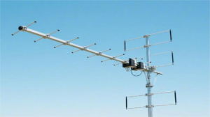
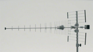
A PCB trace antenna, often etched directly onto the board, is the cheapest option at under 0.30 per unit in 10k quantities and saves vertical space, but it is highly susceptible to noise from nearby components and typically exhibits a radiation efficiency of just 40-60 4.50 BOM cost. For long-range applications, a Yagi is the tool for the job. A 9-element Yagi for 915 MHz can provide 12 dBi of gain, effectively quadrupling the transmission distance compared to a dipole, but it comes with a 60-degree horizontal beamwidth and a physical length of over 500 mm, making it unsuitable for anything but fixed installations. The polarization is another key spec; most consumer devices use linear polarization, but if your device, like a drone, will be rolling and pitching arbitrarily, a helical antenna with circular polarization is mandatory to prevent a 20+ dB fade during maneuvers, albeit at a 30% increase in component cost and a more complex 50-ohm impedance matching network requiring a 3-component LC filter tuned to within ±5% of the center frequency.
Calculate Length and Shape
A half-wave dipole for 2.4 GHz isn’t simply 300 / 2.4 / 2 = 62.5 mm; the velocity factor of bare copper wire (around 0.95) and end effects from the insulators reduce this to approximately 58-60 mm per leg. Getting this length wrong by just 5% can shift the resonant frequency by 120 MHz, moving it completely outside the 2.4 GHz ISM band and collapsing antenna efficiency from over 90% to below 40%. The shape, whether a straight dipole, a folded dipole, or a meandered PCB trace, further modifies the impedance and bandwidth. A meandered trace antenna might compress a 60 mm dipole into a 15 mm x 6 mm area, but this typically reduces bandwidth by 30% and introduces a 15% efficiency loss due to increased resistive losses and unwanted coupling within the meander patterns.
| Antenna Type | Fundamental Formula | Practical Length (L) Adjustment | Key Shape Factor |
|---|---|---|---|
| Half-wave Dipole | L (mm) = 142.6 / f (GHz) | -3% to -5% for velocity factor | Conductor diameter (>1mm ideal) |
| Quarter-wave Monopole | L (mm) = 71.3 / f (GHz) | -4% to -6% for ground plane effect | Ground plane size (min. λ/2 radius) |
| PCB Patch Antenna | L (mm) ≈ 67.8 / f (GHz) / √(εᵣ) | -2% to -4% for fringing fields | Substrate εᵣ (e.g., FR4 ≈ 4.3) |
| 2.4 GHz Helical | C (mm) ≈ 305 / f (GHz) | ±1 turn for fine tuning | Pitch = 0.12λ to 0.18λ |
The most common mistake is using the free-space wavelength formula without accounting for the velocity factor. For a wire dipole, the actual cut length should be 95% of the calculated theoretical length. Always build a prototype longer than needed and plan to trim it iteratively while measuring the return loss.
For a quarter-wave monopole on a ground plane, the starting length is L = λ/4. For 868 MHz, this is 300 / 0.868 / 4 = 86.4 mm. However, the lack of an infinite ground plane shortens the electrical length; on a small PCB with a 50 mm x 50 mm ground plane, the effective length must be reduced by approximately 5%, to around 82 mm, to achieve resonance. The diameter of the conductor significantly impacts bandwidth. A thin 0.5 mm wire for a 433 MHz dipole has a usable bandwidth of about 2 MHz, while increasing the element thickness to 3 mm (e.g., using aluminum tube) can broaden the bandwidth to over 6 MHz, a 300% improvement, by reducing the Q-factor.For a PCB patch antenna, the calculation is more complex. The length (L) of a rectangular patch is approximately L = 0.49 * λ / √(εᵣ), where εᵣ is the substrate’s dielectric constant. For FR4 material (εᵣ ≈ 4.3) at 2.45 GHz, this gives L ≈ 0.49 * 122.4 mm / 2.07 ≈ 29 mm. The width of the patch (W) controls the input impedance; a common rule is W = 1.5 * L, which for this example is about 43.5 mm. The shape of the feed point is critical; feeding at the edge yields an impedance near 200 Ω, while moving the feed inward toward the centerline reduces it. A feed location 8.5 mm from the edge typically provides the standard 50 Ω impedance for a patch of this size.
Consider Your Surroundings
A Wi-Fi antenna perfectly tuned to 2.45 GHz on a test bench can shift down to 2.3 GHz when placed 10 mm from a device’s lithium battery, rendering it ineffective. Signals attenuate at wildly different rates through common materials: a single concrete wall can inflict -15 dB to -20 dB of loss at 2.4 GHz, while a drywall partition may only cause -3 dB to -6 dB. This 14 dB difference is equivalent to a 25x change in signal power, meaning an link that worked at 50 meters in open air might fail after 5 meters indoors. Humidity is another silent killer; a 90% relative humidity level can add an extra 0.5 dB/km attenuation at 24 GHz compared to dry air, which is critical for millimeter-wave links. You must design for the worst-case scenario, not ideal conditions.
- Metal Obstacles: A large metal heatsink or battery placed within λ/4 (30 mm at 2.4 GHz) of a PCB antenna can detune it by over 200 MHz, reduce efficiency by 40%, and create a -10 dB null in the pattern.
- Plastic Enclosures: A common ABS plastic case (εᵣ ≈ 3.0) with a 2 mm wall thickness will capacitively load a antenna, lowering its resonant frequency by approximately 3%.
- Human Presence: A person standing 1 meter from a 3.5 dBi dipole can absorb radiation, creating a shadowing effect that drops signal strength by 15-20 dB and introduces deep fades with 30 dB of fluctuation as they move.
For a 5.8 GHz signal traversing an indoor office, you must account for free-space path loss (-68 dB at 10 meters), plus -6 dB for each drywall wall, and an additional -10 dB margin for furniture and human activity. This predicts a total path loss of -84 dB, which your radio system must overcome. The ground itself creates a reflective plane that causes constructive and destructive interference. For a 1.5-meter-high antenna establishing a 500-meter link, the resulting reflection can cause a +6 dB signal peak or a -20 dB null depending on the exact height and distance, leading to periodic packet loss. To combat this, antenna diversity using two antennas spaced at least λ/2 (60 mm at 2.4 GHz) apart is critical; this spacing ensures a 99% probability that if one antenna is in a null, the other is not, preventing a total link dropout. For devices mounted on vehicles or machinery, vibration is a mechanical killer.
A poorly secured antenna vibrating at a 100 Hz frequency with a 2 mm amplitude will fatigue solder joints, causing a complete failure within 1000 hours of operation. The solution is a mounting base with a damping material or a flexible antenna element that can withstand 5 Gs of acceleration. Finally, for outdoor deployments, UV-resistant radomes are non-negotiable; standard plastics degrade after 18 months of direct sunlight, yellowing and increasing RF loss from 0.2 dB to over 2.0 dB, silently strangling your signal strength.
Build and Check Impedance
Without a proper 50-ohm match, a significant portion of your transmitted power—often 60% or more—reflects back into the transmitter, converting into heat instead of radiated signal. This mismatch doesn’t just reduce range; it can stress power amplifier components, increasing their operating temperature by 20°C and potentially shortening their lifespan by 40%. For a 2.4 GHz Wi-Fi module outputting +20 dBm (100 mW), a 2:1 VSWR (which corresponds to a -10 dB return loss) means 90 mW is delivered to the antenna, a manageable loss. However, a poor 3:1 VSWR (-6 dB return loss) slashes that to just 75 mW, wasting 25 mW and dramatically reducing the effective link margin. Checking and tuning impedance is not optional; it’s what separates a working prototype from a reliable product.
- Vector Network Analyzer (VNA) Essential: A basic $800 VNA can measure S11 (return loss) with ±1.5 dB accuracy up to 3 GHz, revealing if your antenna resonates at the correct frequency. A -10 dB return loss indicates 90% power delivery, while -15 dB or better is the design goal for high-performance systems.
- Matching Network Components: Use 0402 or 0603-size inductors and capacitors with high-Q values (>30 at target frequency) for matching networks. A low-Q (<10) capacitor can introduce 2-3 Ω of parasitic series resistance, sabotaging the match.
- PCB Trace Effects: A 50-ohm microstrip line on 1.6 mm FR4 substrate must be 2.8 mm wide; a miscalculated 2.0 mm trace can present a 65-ohm impedance, creating a mismatch right at the feed point.
For a PCB trace antenna, the connection point is a 0.5 mm wide pad placed 0.2 mm from the antenna element itself; a larger pad or greater distance adds parasitic capacitance that can detune the antenna by 50 MHz. Soldering a coaxial cable directly to a prototype requires a 5 mm long, 0.5 mm wide trace to the antenna feed; a thicker or longer trace will act as an additional inductor, shifting the impedance point upward. When building a wire dipole, the feed point insulation is critical. Using a 2 cm long piece of PVC tubing (εᵣ ≈ 3.0) as a balun instead of a proper ferrite core can add 5 pF of capacitance across the feed, lowering the resonant frequency by 3%. Once built, connect the VNA and measure the S11 parameter. The goal is a clear dip on the Smith chart reaching the center (50-ohm point) at your target frequency. If the impedance point is in the top half of the chart (e.g., 30 + j25 Ω), it indicates excessive inductance; you must add a series capacitor or a shunt inductor to cancel it out.A value of 1.2 pF in series or a 8.2 nH shunt inductor might be needed for a 2.4 GHz match. If the point is in the bottom half (e.g., 70 – j40 Ω), it shows excessive capacitance, requiring a series inductor or shunt capacitor, such as a 5.6 nH series coil. Always use a simulation tool to calculate the initial component values, but expect to manually tune them by swapping parts.
Test and Adjust Performance
Without this data, you’re guessing. A antenna measuring a perfect -25 dB return loss on a VNA could still have a radiation efficiency of only 40% due to nearby lossy materials, effectively wasting over half of your transmit power as heat. A 3 dBi gain spec means nothing if the radiation pattern has a -15 dB null directly in the path to your receiver, causing a 97% drop in signal strength at that angle. Performance testing involves three key metrics: total radiated power (TRP), which quantifies how much power actually leaves the system; total isotropic sensitivity (TIS), which measures receiving capability; and the 3D radiation pattern, which maps signal strength in all directions.
- Radiation Pattern Measurement: Use an antenna test range or a simple turntable to plot gain every 15 degrees in azimuth and elevation. Identify nulls deeper than -10 dB that could kill your link.
- Efficiency Measurement: A $15,000 reverberation chamber provides the most accurate results, but a calibrated reference antenna and a 3-meter flight cable can give efficiency within ±10% accuracy.
- Real-world Range Test: Conduct a 1 km line-of-sight test, measuring packet error rate (PER) at -95 dBm receive power. A PER below 1% validates the entire RF chain.
The most critical test is measuring the 3D radiation pattern. This reveals if that 5 dBi gain is focused in a useful direction or wasted. Mount the prototype on a programmable turntable in an open field or anechoic chamber. Transmit a continuous wave signal and use a calibrated spectrum analyzer with a reference antenna positioned 5 meters away. Rotate the device 360 degrees in 15-degree increments, recording the received power at each point. This will reveal the beamwidth; a good omnidirectional antenna should have less than ±3 dB variation in the horizontal plane.
A variation exceeding 6 dB indicates pattern distortion, often from a nearby battery or display cable. Next, measure efficiency using the gain substitution method. Replace your prototype with a standard gain horn antenna with a known gain of 10.0 dBi. Measure the difference in received power; if your antenna produces a signal 7 dB weaker, its gain is approximately 3 dBi. To find efficiency, compare this measured gain to the simulated directivity. Finally, conduct a bit error rate (BER) test over distance. Place your complete product in its final housing 50 meters from the receiver. Transmit a 1 Mbps data stream and measure the BER while lowering the transmit power. A well-designed system should achieve a 10⁻⁶ BER (1 error per million bits) at a receive power level of -85 dBm. If the BER spikes at -75 dBm, the issue is likely noise from your device’s own digital circuitry interfering with the receiver, requiring better shielding or filter components on the power lines. Each test iteration should inform a physical adjustment: bending a monopole element 3 mm to shift resonance, adding a 2 mm thick grounded aluminum foil shield to block noise from a processor, or applying a 0.5 mm thick RF absorber patch to a plastic case to dampen surface waves that distort the pattern.
Never finalize a design based solely on return loss. An antenna can have a perfect 50-ohm match but be a terrible radiator. Always validate with at least a basic radiation pattern and efficiency measurement before mass production. The most common failure is neglecting to test the device in its final assembled state with all components powered.