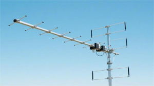
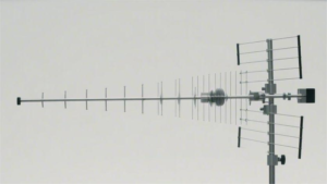
Leveraging our deep accumulation of RF technology, we provide customized 5G antenna solutions.
By utilizing an advanced 4×4 MIMO architecture and supporting millimeter-wave (mmWave) bands, we achieve peak throughput exceeding 10Gbps and extreme latency below 1ms, ensuring absolute reliability and data integrity in high-bandwidth industrial interconnection scenarios.
Table of Contents
High Bandwidth Optimization
In the 5G Sub-6GHz band, through 4×4 MIMO and 256-QAM modulation, single-sector throughput can reach 1.5Gbps;
In the millimeter-wave band, utilizing 800MHz of continuous bandwidth, peak rates can exceed 10Gbps.
We maintain antenna isolation above 20dB and control return loss below -10dB. Combined with LCP low-loss materials (Df value of 0.002), we effectively reduce transmission loss by 0.5dB per centimeter in the 28GHz band, ensuring stable downlink rates under high-density connections.
Frequency Band Expansion
To achieve full coverage from 600MHz to 7.125GHz within the Sub-6GHz band, antenna engineers must employ multi-resonance mode designs.
Traditional single-resonance antenna bandwidth is usually only 5% to 10% of the center frequency, which cannot meet the broadband requirements of 5G New Radio (NR).
By introducing parasitic elements and aperture tuning techniques, we can generate multiple resonance loops on the Smith chart, controlling the system’s Voltage Standing Wave Ratio (VSWR) within 3:1 in the low-frequency band (617MHz to 960MHz), and within 2:1 or even lower in the mid-to-high frequency bands (1.7GHz to 5GHz).
This wideband design allows a single physical antenna unit to simultaneously transmit wide-area control signals through low-frequency bands and perform high-speed data throughput via mid-to-high frequency bands. This eliminates the need to stack excessive single-band antennas inside the device, thereby leaving physical space for 4×4 MIMO or even 8×8 MIMO layouts.
In the C-Band spectrum (3.3GHz to 4.2GHz), to acquire continuous channel bandwidths of 100MHz or even 200MHz, the antenna’s Q value must be strictly compressed. Broad monopoles or slot antenna structures are typically used to increase the surface current path width of the radiator, reducing the ratio of stored energy to radiated energy and achieving inherent broadband characteristics at the physical layer.
When a device needs to aggregate a low-frequency carrier (e.g., 700MHz, Band n12) and a mid-frequency carrier (e.g., 3.7GHz, Band n77), the wavelengths of the two bands differ vastly, leading to completely different current distributions on the same antenna aperture.
To support this Inter-band Carrier Aggregation (Inter-band CA), the RF front-end module (RFFE) must provide more than 30dB of isolation between the two receive paths to prevent intermodulation products of the transmit signal from falling into the receive band, which would raise the noise floor and lower the Signal-to-Noise Ratio (SNR).
In the downlink, by aggregating 3 or 4 Component Carriers (CCs)—for example, one 20MHz low-frequency carrier plus three 100MHz mid-frequency carriers—the total available bandwidth can instantly reach 320MHz.
Under this configuration, even with basic 64-QAM modulation, a downlink rate of 2Gbps can easily be achieved.
In uplink optimization, utilizing UL Tx Switching technology, the device can rapidly switch transmit channels between low-frequency FDD and mid-frequency TDD carriers based on signal quality, ensuring high-bandwidth upload capabilities even at the cell edge.
In the FR2 frequency range (e.g., n258 band at 24.25-27.5GHz), the bandwidth of a single component carrier starts at 50MHz and can reach a maximum of 400MHz.
By aggregating 8 such carriers, the continuous bandwidth available to the physical layer is as high as 800MHz or even over 1.2GHz.
This extremely wide spectrum pipe allows 5G networks to carry uncompressed 4K/8K video streams or VR content.
However, the wavelength of millimeter waves is only on the millimeter scale, resulting in extremely high path loss and high susceptibility to blockage by the human body or glass.
To utilize this 800MHz bandwidth, phased array antenna technology must be used, integrating 4-unit, 8-unit, or even 16-unit antenna arrays within a package the size of a fingernail.
These arrays form high-gain directional beams (typically exceeding 25dBi) by adjusting the phase offset of each unit to compensate for air propagation loss.
To maintain the stability of high-bandwidth transmission, mmWave modules are typically distributed across three different sides of the device (e.g., top, left, and right) and communicate with the baseband processor via Intermediate Frequency (IF) signals.
When a hand blocks the right-side module causing bandwidth to drop, the system activates the top or left module within microseconds to ensure continuous high throughput.
In this process, the choice of PCB material is critical.
Liquid Crystal Polymer (LCP) or other fluoride-based substrates with low dielectric constants (Dk < 3.0) and extremely low loss factors (Df < 0.003) must be used.
This is because, at 28GHz, standard FR-4 materials would cause signal attenuation of more than 2dB per inch, directly consuming valuable bandwidth gains.
Material Loss
In 5G RF system design, signal frequencies jump from the traditional 2GHz to 28GHz or even 39GHz, which causes the energy dissipation of electromagnetic waves through circuit board substrates to increase geometrically.
To support the SNR required for high bandwidth, the performance of the material’s dielectric constant (Dk) and dissipation factor (Df) determines final system efficiency.
In a 2.4GHz environment, standard FR-4 epoxy resin materials perform adequately, with Df values typically around 0.015.
However, once the frequency reaches the 28GHz mmWave band, the signal attenuation of FR-4 exceeds 1dB per inch, with most energy disappearing as heat along the transmission path.
To solve this, hardware architectures are shifting on a large scale toward low-loss materials, focusing on pushing the Df value below 0.003.
Liquid Crystal Polymer (LCP) is currently the recognized fundamental choice.
Across an extremely wide frequency range from 1GHz to 100GHz, its Dk value remains stable at around 2.9, while the Df value stays near 0.002.
This electrical stability ensures that the resonant frequency of the antenna does not shift under a continuous 400MHz bandwidth, preventing signal distortion caused by material thermal expansion/contraction or frequency drift.
| Material Type | Dk at 10GHz | Df at 10GHz | 28GHz Trans. Loss (dB/inch) | Water Absorption (%) | Applicable Band |
|---|---|---|---|---|---|
| Standard FR-4 | 4.4 | 0.018 | > 1.2 | 0.30 | < 3GHz |
| MPI (Modified PI) | 3.1 | 0.004 | 0.5 – 0.7 | 0.15 | Sub-6GHz |
| LCP (Liquid Crystal Polymer) | 2.9 | 0.002 | 0.2 – 0.3 | 0.04 | mmWave |
| PTFE (Teflon) | 2.1 | 0.001 | 0.1 – 0.15 | < 0.01 | Satellite/EHF |
Because the Dk value of water molecules is as high as 80 and they possess extremely high loss, any moisture absorbed by the substrate will significantly raise the circuit’s equivalent Df value.
The water absorption rate of LCP material is only 0.04%, allowing it to maintain the stability of 5G mmWave links even in humid outdoor environments.
In contrast, traditional polyimide (PI) has a water absorption rate exceeding 0.3% in the same environment, leading to an additional signal attenuation of more than 0.5dB at 28GHz.
For devices needing to aggregate multiple carriers to reach 5Gbps rates, this 0.5dB difference often determines whether the link is forced to downgrade to a lower-order modulation due to insufficient SNR.
At 28GHz, the skin depth of copper is only 0.38 microns.
If rough electrodeposited (ED) copper foil is used to enhance the bond between the foil and substrate—with Rz roughness typically between 3 to 5 microns—it far exceeds the skin depth.
This roughness causes the actual flow path of the current to lengthen, thereby increasing impedance loss.
Designs must adopt Rolled Annealed (RA) copper or Very Low Profile (VLP) copper foil to control surface roughness within 1.5 microns, which can reduce 28GHz transmission loss by an additional 20% to 30%.
This quantitative control over material details is the foundation for maintaining stable throughput across an 800MHz ultra-wide bandwidth.
In the multilayer board integration process, material matching also involves a balance between thermal performance and mechanical stability:
- CTE Matching: The Coefficient of Thermal Expansion (CTE) of LCP can be adjusted through production processes to around 17 ppm/°C, perfectly matching copper foil to prevent interlayer delamination in high-heat 5G base station environments.
- Dielectric Thickness Control: To maintain a characteristic impedance of 50 ohms, ultra-thin dielectric layers of 2 mil or 1 mil are typically used in high-frequency bands, requiring the material to possess high tensile strength.
- Solder Mask Impact: Traditional green solder mask ink has extremely high loss in the mmWave band. In high-bandwidth antenna radiation areas, windows must be opened in the mask, or specialized low-loss photosensitive inks must be used.
- Flexible Connection Needs: In foldable or miniaturized 5G devices, MPI plays the role of a more cost-effective solution for mid-band carrier aggregation links due to its better bending fatigue life.
Low-Temperature Co-fired Ceramic (LTCC) exhibits excellent Q values in bands above 30GHz, enabling extremely narrow beam steering, which is highly effective for mmWave high-gain requirements.
The Dk value of LTCC is typically between 5 and 10. A higher Dk aids in the miniaturization of antenna units.
By embedding filter circuits within multiple ceramic layers, a 16-unit array can be integrated within a 10mm square area.
High-performance 5G hardware requires that after a “Double 85” test (85 degrees Celsius, 85% humidity), the Dk value shift must not exceed 1%.
This strict requirement ensures that after five years of service, the device can still accurately lock onto the new Wi-Fi 6E/7 bands from 5.925GHz to 7.125GHz, without antenna detuning caused by material degradation leading to unnecessary retransmissions and latency.
Spatial Multiplexing Capability
In the actual operation of 5G communication systems, spatial multiplexing capability allows base stations and terminals to send multiple independent data streams on the exact same frequency and time resources.
This is not achieved by increasing spectrum width, but by utilizing the multi-path effect of radio waves during spatial propagation.
When a signal is emitted from an antenna, it undergoes reflection from buildings, the ground, or indoor furniture, forming multiple arrival paths.
If the antenna array can distinguish the physical differences between these paths, the spectral efficiency can be multiplied.
For example, in a 4×4 MIMO configuration, the base station transmits using four antennas and the terminal receives using four.
If the spatial environment is sufficiently complex and the SNR is maintained above 25dB, the system can transmit four layers of data simultaneously.
In the millimeter-wave band, this capability is even more pronounced. As wavelengths shorten, more antenna units can be accommodated within a smaller physical size, making concurrent data across sixteen or even thirty-two layers possible.
Spatial multiplexing relies on the rank of the channel matrix; the higher the rank, the more independent channels exist in space. In an open suburban environment, signal paths are singular, and the rank is usually only 1, meaning only one data copy can be sent regardless of the number of antennas. However, in dense urban areas like Manhattan, signals reflect multiple times, and the rank can easily reach 4 or higher.
By deploying 64T64R (64 transmit, 64 receive) Active Antenna Units (AAU), base stations no longer broadcast signals to an entire sector in the traditional way.
Instead, they use digital weight adjustments to divide the space into multiple extremely narrow beams.
Each beam can be assigned to a different user; this is Multi-User MIMO (MU-MIMO).
In large stadiums or busy European transportation hubs, a base station can simultaneously provide independent downlink data streams to 16 different users, with each user receiving near-peak bandwidth.
This approach increases the total throughput of the entire cell by more than 10 times without requiring additional expensive spectrum.
To maintain this efficiency, the system performs channel estimation thousands of times per second.
Through codebook information fed back by the terminal, it adjusts the antenna array’s transmission parameters in real-time, ensuring that signal interference between different users remains below -15dB.
In actual Fixed Wireless Access (FWA) scenarios, if a terminal is installed at a window and equipped with 4 high-gain antennas, the spatial multiplexing order can remain stable at 4 layers even 2 kilometers from the base station. Empirical data shows that in this state, single-user downlink stable rates can be maintained between 1.2Gbps and 1.8Gbps.
Multiple sets of cross-polarized antennas must be arranged within a phone’s frame—usually two vertically polarized and two horizontally polarized—to use the different polarization directions to increase signal independence.
Since hand blockage can degrade some antenna performance, modern 5G terminals typically feature 6 to 8 built-in antennas.
The baseband chip automatically selects the 4 best-performing ones for combination based on Channel Quality Indicators (CQI).
In cases of poor SNR, the system will actively reduce the multiplexing layers from 4 to 2 or 1 and switch to a more robust modulation method, sacrificing speed for connection continuity.
Spatial correlation is the primary obstacle to multiplexing capability. If the distance between antennas is less than half a wavelength, correlation between signals increases significantly, making it impossible to effectively separate data streams. In the 3.5GHz band of Sub-6GHz, half a wavelength is approximately 4.3 cm, which imposes strict isolation requirements on antenna layouts in miniaturized devices.
Base stations use Zero-forcing technology to produce signal nulls in the direction of non-target users, thereby eliminating mutual crosstalk between multiple users.
In the mmWave band, because beams are extremely narrow, spatial isolation can exceed 20dB, making frequency reuse very efficient.
When the base station detects that two users are separated by more than 10 degrees in physical space, it will allocate the same frequency resources for concurrent transmission.
This refined management of the spatial dimension allows 5G networks to support a connection density of one million devices per square kilometer.
In actual deployment tests, by optimizing spatial multiplexing parameters, the uplink bandwidth of the base station also gains significant growth.
Through a 2×2 MIMO architecture, a phone’s upload speed can be increased from a base of 125Mbps to over 250Mbps, meeting the demand for high bandwidth in HD live streaming and cloud backups.
Interference Cancellation and Combining (IRC) technology on the terminal side is equally important. By performing complex mathematical operations on the multiple received signals, it can accurately extract its own data layers from messy background noise. In signal edge areas, this technology can increase the actual available bandwidth level by 30% to 50%.
Coordination at the material level also directly contributes to spatial multiplexing.
To ensure phase consistency across multiple antenna paths, PCB traces must be strictly equal in length, and the dielectric material’s electrical performance drift across different temperatures must be minimal.
If the dielectric constant fluctuates wildly with temperature, it will cause the beam direction to deviate from the intended position, destroying the layer isolation of spatial multiplexing.
Using low-loss, high-thermal-stability LCP materials ensures that in high-summer temperatures, the pointing deviation of the antenna array is controlled within 1 degree.
This precision at the hardware level directly guarantees the decoupling capability of large-scale antenna groups in multi-path environments.
This end-to-end physical layer optimization allows 5G to handle spatial signals like physical entities, pushing radio resource utilization to the edge of the Shannon limit.
Advanced MIMO Technology
Advanced MIMO increases spectral efficiency by fivefold through 64-channel or 128-channel arrays.
In the Sub-6GHz band, it supports single-sector throughput of over 5Gbps.
Relying on high-gain beams of 15 to 20dBi, vertical coverage is expanded by 25 degrees, and it can simultaneously handle 16 independent spatial streams, increasing signal strength at the cell edge by more than 10dB.
Array Scale & Hardware Integration
A standard 64T64R Active Antenna Unit (AAU) typically integrates 192 dual-polarized oscillator units internally, arranged in a 3×4 sub-array on a baseplate 800 mm long and 400 mm wide.
In the 3.5GHz band, the physical spacing between adjacent antenna units is strictly set between 42 mm and 45 mm—maintaining approximately half a wavelength to reduce sidelobe interference during the spatial beamforming process.
An array of this scale can support 64 RF channels, each controlled via independent phase shifters and power amplifiers.
In the vertical structure of hardware integration, modern 5G base station equipment has abandoned traditional remote radio head (RRH) architectures in favor of systems that combine the RF front-end with the antenna array.
RF boards typically use 12- to 16-layer high-frequency multilayer PCB stacks, with substrates chosen from PTFE-type materials that have a dielectric constant (Dk) stable around 3.0 and a dissipation factor (Df) below 0.0015.
Every RF channel includes a set of high-efficiency Gallium Nitride (GaN) power amplifiers, whose drain efficiency can reach 45% to 50% in the 3.5GHz band.
- Physical Weight and Wind Resistance: The total unit weight is typically controlled between 22 kg and 25 kg. To operate long-term on towers in North America or Western Europe, the enclosure’s heat sink design must withstand instantaneous wind speeds of 200 km/h.
- Digital Beamforming Components: Internally integrated Large-Scale ASICs handle baseband data streams of 40Gbps per second and split signals into 64 paths for digital-to-analog conversion (DAC), with quantization bits typically maintained at 12 or 14 bits.
- Bandpass Filter Integration: To achieve good out-of-band rejection in the n78 or n77 bands, the system integrates ceramic dielectric filters, with insertion loss pressed below 1.0dB and rejection capability greater than 40dB at 20MHz from the center frequency.
With the introduction of mmWave bands (e.g., n258 band), the array scale further compresses to 256 or 512 antenna units, but the overall size shrinks to a 200 mm square.
This high-density hardware arrangement requires RF chips and antenna patches to be combined via Antenna-in-Package (AiP) technology.
The cooling system at this stage uses a combination of active heat pipes and die-cast aluminum alloy fins, with fin spacing maintained at 3 mm to 5 mm to ensure that at an ambient temperature of 50 degrees Celsius, the junction temperature of internal power amplifiers does not exceed 125 degrees Celsius.
The power management module must provide multiple low-voltage, high-current outputs under a 48V DC input, with the power amplifier supply current reaching over 30 Amperes at peak.
To ensure high consistency in phase and amplitude across these 192 units, hardware calibration parameters are written into flash memory before leaving the factory.
- Phase Accuracy Control: The phase error for each channel must be controlled within ±5 degrees, and the amplitude error within 0.5dB.
- Interface Protocol Standards: The interface between baseband and RF uses the eCPRI protocol, exchanging data via 25Gbps fiber interfaces and supporting carrier bandwidths up to 200MHz.
- Lightning Protection and EMC: DC ports must have a 20kA surge protection capability. The entire unit complies with European EMC standards such as EN 301 489, ensuring no bit errors occur in electromagnetic environments near high-voltage lines or broadcast towers.
In actual RF links, the noise figure of the Low Noise Amplifier (LNA) is key to guaranteeing weak signal reception.
GaAs LNAs are typically chosen, with noise figures controlled between 1.5dB and 1.8dB.
When signals reach the cell edge 2 kilometers away, the receiver can still extract valid QAM signal streams from the background thermal noise.
For customized small cell solutions, hardware integration tends toward more compact SoC solutions, integrating the IF, transceiver, and part of the baseband processing functions into a single 40 mm square chip, reducing total power consumption to below 150 watts.
The directional gain of a 64-element antenna is generally between 22dBi and 24dBi.
In high-rise building coverage scenarios, by adjusting the phase offset of each row of units in the array, the hardware system can generate dynamic beams with a vertical scanning width of 30 degrees.
This flexibility avoids the trouble of traditional mechanical antennas needing manual tilt adjustments.
In terms of structural connection, hundreds of blind-mate connectors or pogo pins are used between the array backplane and the RF board, with contact pressure maintained above 0.5 Newtons to prevent intermodulation interference caused by poor contact in long-term vibration environments.
Precise Beam Pointing Control
In a standard 64-channel Massive MIMO base station, the baseband processing unit needs to complete hundreds of millions of complex matrix operations per second to assign independent weight vectors to each RF channel.
These weight vectors consist of real and imaginary parts, controlling signal delay offsets on the sub-nanosecond scale.
When 192 antenna units transmit signals synchronously, the main lobe width is compressed to between 7 and 10 degrees horizontally, with highly concentrated energy.
This energy aggregation effect compensates for path loss during transmission. Compared to traditional 120-degree sector broadcast antennas, directional gain can typically be increased by an additional 15dBi to 20dBi.
The horizontal scanning range of the signal in the 3.5GHz band reaches 120 degrees. The dynamic adjustment range in the vertical dimension is between ±15 degrees.
When handling coverage needs for high-rise apartment buildings or multi-story office buildings, the system can simultaneously generate multiple beams that overlap in vertical height but do not interfere with each other.
By adjusting the phase difference of vertically arranged elements, the beam can accurately scan from the ground floor lobby to heights over 200 meters.
On the hardware implementation level, the system uses specially designed RF ASICs that integrate high-speed digital converters and low-latency phased array controllers.
At a carrier bandwidth of 100MHz, the beam weight update frequency is typically set to once every 0.5 milliseconds, enabling adaptation to vehicular mobile scenarios at speeds over 120 km/h.
To prevent severe signal fluctuations during movement, the system introduces beam tracking algorithms, using historical position data to predict the optimal beam direction for the next moment.
This approach effectively reduces the risk of disconnection caused by beam switching, controlling switching latency within 10 milliseconds.
In deployments at European transport hubs, a single base station can simultaneously maintain more than 16 high-gain independent beams, providing dedicated data channels for users in different locations.
Energy concentration improves the SNR at the cell edge by 6dB to 9dB. Single-user peak downlink rates can still be maintained above 1.5Gbps in interference environments.
Through zero-forcing technology, the antenna system can actively form “dark zones” of extremely low signal strength in the direction of interference sources, with suppression levels typically dropping below 20dB of the main lobe energy.
In Multi-User MIMO scenarios, when two users are physically close, the system utilizes the principle of spatial orthogonality to calculate two sets of non-overlapping precoding weights through complex algorithms.
This allows the base station to transmit data to multiple terminals on the same frequency resource simultaneously without significant co-channel interference.
In actual test data, this spatial multiplexing technology increases spectral efficiency by 3 to 5 times.
For customized mmWave antennas, due to shorter wavelengths and higher integration density of antenna elements, beams can be further refined into ultra-narrow beams of about 3 degrees.
The system’s beam switching speed is better than 5 milliseconds. Spatial isolation within a 500-meter range is maintained above 25dB.
The installation tolerance of each radiator patch is limited to within 0.1 mm to ensure the accuracy of phase offset calculations.
Internal RF links use low-power, high-linearity power amplifiers to ensure the signal does not produce significant non-linear distortion during phase shifting.
Under a Software-Defined Networking (SDN) architecture, beam width and direction can be dynamically scaled based on real-time traffic distribution.
When user density in a specific area suddenly increases, the base station automatically splits wide beams into multiple narrow beams, thereby increasing the connection capacity of that area.
This automated beam management system reduces the cost of manually adjusting antenna mechanical tilt.
In industrial automation scenarios, this technology is responsible for providing stable wireless links for mobile robots.
Even when robots are in environments shielded by dense metal equipment, the system can reconstruct signal paths within 1 millisecond by searching for optimal reflection paths, ensuring the determinism of instruction transmission.
Customized Antenna Isolation Parameters
For 64-channel or 128-channel Massive MIMO systems, co-channel interference shielding capability needs to reach between 25dB and 30dB to ensure that the Envelope Correlation Coefficient (ECC) between physical channels remains below 0.1.
In Sub-6GHz RF front-end integration, designers typically introduce parasitic decoupling elements or neutralization line structures between adjacent radiation units to cancel out induction signals generated by spatial electromagnetic coupling via offsetting currents.
This physical-layer refinement allows the antenna to maintain a port-to-port return loss better than 15dB within an operating bandwidth of 100MHz or even 200MHz, while improving Cross-Polarization Discrimination (XPD) to over 20dB.
In urban macro-site deployments in North America and Europe, this high-isolation design effectively suppresses inter-branch interference caused by multi-path reflections, lowering the receiver’s noise floor by 2dB to 3dB.
| Isolation Indicator (dB) | Data Stream Independence (ECC) | System Throughput Gain | Typical Application Scenario |
|---|---|---|---|
| 15dB – 20dB | 0.3 – 0.5 | Base Level | Suburban and low-density areas |
| 25dB – 28dB | 0.05 – 0.1 | 20% Increase | High-density urban 5G macro sites |
| Above 30dB | Better than 0.02 | 35% Increase | Industry 4.0 indoor ultra-reliable links |
In the 3.5GHz band, the center spacing of adjacent radiation patches is typically set at around 43 mm.
By embedding Defect Ground Structures (DGS) in the PCB trace layer, induced current paths on the ground plane can be cut off, improving isolation by 5dB without increasing antenna volume.
The selection of low-loss PTFE substrates is critical; fluctuations in the dielectric constant between 2.2 and 3.5 must be less than 0.02, ensuring phase consistency of all 192 antenna units in wide-temperature environments.
In the manufacturing phase, the RF feed network is fine-tuned via laser trimming to control the VSWR below 1.5, reducing energy back-reflection at interfaces and providing a clean physical channel environment for high-order QAM modulation schemes.
RF circuit boards typically use 12- to 18-layer high-frequency stack architectures, with dense ground via arrays arranged on both sides of key signal lines to form miniature electromagnetic shielding chambers.
This design pushes the signal isolation between different polarization directions toward the 32dB limit.
For customized small cells supporting 2×2 or 4×4 MIMO, to achieve peak rates over 1Gbps, the integrated dielectric filters must reach an out-of-band rejection capability of around 40dB to prevent carrier leakage from adjacent bands from entering the sensitive LNA front-end.
In actual link budget calculations, every 3dB improvement in isolation can increase the average spectral efficiency of a single cell by approximately 15% under the same transmit power.
| Material Property Parameter | Indicator Value | Impact on Isolation | Performance Result |
|---|---|---|---|
| Dk Stability | ± 0.05 | Affects phase center deviation | Reduces beam pointing error |
| Dissipation Factor (Df) | 0.0009 – 0.0015 | Affects total RF link loss | Improves antenna radiation efficiency |
| Copper Foil Roughness (Rz) | Below 2 microns | Affects skin effect loss | Improves gain consistency at high frequencies |
In high-frequency applications like 28GHz mmWave, as wavelengths shorten to the millimeter scale, isolation faces even tougher challenges.
By adopting Antenna-in-Package (AiP) technology, antenna oscillators are directly integrated on top of the RF chip.
Utilizing the micro-gap layout of multilayer organic substrates, an extremely high integration of 256 units can be achieved in an area of only 10 mm square.
At this point, the system uses Electromagnetic Band Gap (EBG) structures to suppress surface waves.
These artificial electromagnetic materials can form “photonic band gaps” within specific frequency bands, preventing unnecessary signal leakage between adjacent units.
Test data in laboratory environments show that this 3D spatial isolation technology allows the amplitude difference between the main lobe and the first sidelobe to be maintained above 18dB, enabling more accurate spatial partitioning during beamforming and supporting a greater number of concurrent UEs for collision-free communication.
Ultra-Low Latency Design
This design is based on the 3GPP R16 standard, setting the Sub-Carrier Spacing (SCS) to 60kHz, which shortens the length of a single slot to 0.25 milliseconds.
With 256-QAM modulation and 100MHz of continuous carrier bandwidth, physical layer air interface latency can be stabilized below 1 millisecond.
Using low-loss LCP substrates, link jitter is controlled at the 50-microsecond level.
Combined with a 4×4 MIMO array, this reduces retransmission overhead caused by signal collisions, meeting the feedback speed requirements for real-time operation of remote equipment.
Physical Link Optimization
In the 28GHz band, the free-space wavelength is approximately 10.7 mm, while in a PCB material with a dielectric constant of 3.5, the effective wavelength shortens to about 5.7 mm.
If the trace error from the antenna feed point to the RF chip reaches 0.5 mm, it creates a significant phase shift, causing beamforming accuracy to drop.
To achieve sub-millisecond air interface latency, physical link routing lengths are typically restricted to within 5 mm, and traces are required to use equal-length differential designs, with length tolerances controlled within 0.02 mm.
This extremely high processing precision prevents microsecond-level deviations in signal arrival times across different channels, ensuring the demodulation algorithm can lock onto payload data immediately.
From the perspective of electromagnetic wave propagation, signal transmission speed in a medium is inversely proportional to the square root of the material’s dielectric constant (Dk).
When using traditional FR-4 substrates, the dielectric constant fluctuates significantly with temperature, easily causing instability in signal transmission speed.
In contrast, choosing Liquid Crystal Polymer (LCP) or PTFE substrates can stabilize the dielectric constant between 2.9 and 3.1.
In 39GHz mmWave applications, the dissipation factor (Df) of LCP material is typically below 0.002, reducing electromagnetic energy attenuation along the transmission path, allowing the RF Power Amplifier (PA) to use smaller gains to reach the intended coverage.
The table below shows the specific impact of physical link parameters on signal transmission at different frequencies:
| Frequency (GHz) | Dielectric Material | Dielectric Constant (Dk) | Dissipation Factor (Df) | Insertion Loss per cm (dB) | Rec. Max Trace Length (mm) |
|---|---|---|---|---|---|
| 3.5 | Advanced FR-4 | 4.2 | 0.015 | 0.25 | 25.0 |
| 28 | Fiberglass PTFE | 3.0 | 0.0015 | 0.85 | 6.5 |
| 39 | LCP (Liquid Crystal Poly.) | 2.9 | 0.0018 | 1.15 | 4.2 |
| 60 | Ceramic Filled PTFE | 3.2 | 0.0012 | 1.95 | 2.8 |
In 5G high-frequency bands, current flows almost exclusively in an extremely thin surface layer of the conductor; the skin depth at 28GHz is only 0.39 microns.
If the copper foil surface roughness is too high, the charge flow path is forced to bend along the uneven surface, effectively increasing the wire’s impedance and lengthening the electron’s travel path.
Adopting Hyper-Very Low Profile (HVLP) copper foil can reduce this additional latency caused by increased impedance by more than 15%.
Simultaneously, the design form of the transmission line also changes signal energy distribution.
Coplanar Waveguide (CPW) structures, by providing better shielding between ground and signal lines, are more suitable for compact layouts than microstrip lines and perform better in reducing parasitic inductance, allowing signals to maintain waveform integrity through impedance transformers.
When a signal enters inner layers from surface traces for processing, vias generate parasitic capacitance. If poorly handled, this causes impedance discontinuities.
Back-drilling technology is typically used to remove extra metal stubs in vias, preventing stubs from creating resonant interference.
A via with a 0.2 mm diameter, if not optimized, can produce more than 2dB of return loss at 28GHz, whereas precision-designed controlled-impedance vias can keep return loss below -20dB.
| Link Component | Common Issue | Optimization Goal | Optimized Performance |
|---|---|---|---|
| SMPM Connector | Impedance Mismatch | VSWR | Below 1.25 |
| Via Stubs | Parasitic Resonance | Stub Length | Less than 0.1 mm |
| Differential Traces | Phase Inconsistency | Skew | Below 2 picoseconds |
| Shield Solder | Cavity Resonance | Resonant Freq (f0) | > 2x Signal Bandwidth |
The output impedance of semiconductor devices drifts as temperature rises, causing mismatch in a previously tuned 50-ohm circuit.
By embedding thermally conductive ceramic gaskets or nano-carbon heat dissipation materials at the base of antenna brackets, the operating temperature of the RF chip can be held below 65 degrees Celsius, preventing increased phase noise due to temperature.
Aggravated phase noise forces the baseband processor to increase the length of error-correcting codes, generating tens of milliseconds of additional algorithmic latency.
To achieve cooperative operation of multi-antenna arrays, the attenuation consistency of each physical branch must be maintained within 0.2dB.
In a 64T64R Massive MIMO system, this consistency ensures that the spatial multiplexing algorithm has an extremely high SNR during channel estimation.
By using high-isolation layout solutions at the physical layer—controlling crosstalk between adjacent channels below -35dB—frequent retransmissions at the logical link layer can be eliminated from the source, allowing data streams to travel through the wireless link as smoothly as through optical fiber.
Frame Structure Fine-Tuning
Traditional communication standards typically use a fixed Sub-Carrier Spacing (SCS), such as 15kHz, resulting in a fixed transmission slot length of 1 millisecond.
In scenarios requiring extremely low latency, a 1ms wait time often fails to meet real-time feedback requirements.
The 5G NR (New Radio) standard introduces a flexible scaling mechanism, compressing the symbol length in the time domain by increasing sub-carrier spacing.
When SCS is increased to 30kHz, the slot length is halved to 0.5 milliseconds;
In the 120kHz spacing commonly used for mmWave, the slot length is drastically compressed to 0.125 milliseconds.
In standard mode, the system needs to accumulate 14 OFDM symbols to complete one scheduling cycle.
Non-slot scheduling, however, allows data streams to begin transmission at any symbol position in the middle of a slot, supporting mini-slots of 2, 4, or 7 symbols.
For industrial control instructions of only a few dozen bytes, using a 2-symbol mini-slot can complete air interface transmission within 33 microseconds, without waiting for the remaining symbol positions.
| Parameter | 15kHz (u=0) | 30kHz (u=1) | 60kHz (u=2) | 120kHz (u=3) |
|---|---|---|---|---|
| Single Symbol Duration | 66.7 μs | 33.3 μs | 16.7 μs | 8.33 μs |
| Slot Length (14 Symbols) | 1.0 ms | 0.5 ms | 0.25 ms | 0.125 ms |
| Max Mini-slot Duration | 143 μs | 71.5 μs | 35.7 μs | 17.8 μs |
| Slots per Frame | 10 | 20 | 40 | 80 |
Regarding duplex mode fine-tuning, the Self-contained slot structure achieves downlink data transmission, guard period switching, and uplink acknowledgment feedback (ACK/NACK) within the same 0.5ms or shorter slot.
This structure eliminates the logic of waiting across slots for feedback, shortening the Round Trip Time (RTT) of Hybrid Automatic Repeat Request (HARQ) to within 250 microseconds.
When a receiver detects a data error, the extremely short feedback loop allows the physical layer to initiate a retransmission immediately in the next adjacent slot. This rapid response mechanism is critical for maintaining 99.999% link reliability.
Beyond time-axis compression, Configured Grant technology eliminates handshake latency brought by traditional request-response mechanisms through resource reservation strategies.
In standard flows, a terminal device needs to send a Scheduling Request (SR) before sending data, wait for the base station to issue an Uplink Grant, report a Buffer Status Report (BSR), and finally start transmitting data.
This series of round trips generates a fixed latency of 3 to 8 milliseconds.
Using the Configured Grant mode, the base station pre-allocates periodic physical resource blocks to specific devices. Once data is generated, the device can send it directly at the nearest resource position without a request.
- Signaling Overhead Reduction: Eliminates the SR and BSR handshake stages, directly saving approximately 4.5 milliseconds of initial access latency.
- Resource Pre-allocation Cycle: Common configuration cycles are 1 slot or 2 symbols, ensuring the wait time after data arrival is below 50 microseconds.
- Retransmission Enhancement: Supports multiple blind retransmissions on configured grant resources without waiting for explicit feedback from the base station, improving the first-packet arrival rate through spatial and temporal diversity.
- Priority Pre-emption: When high-priority, latency-sensitive data (such as collision warnings) is generated, the system supports automatically suspending ongoing broadband services to ensure high-priority bitstreams take precedence on the spectrum.
In complex spectrum environments, the Pre-emption mechanism in the downlink allows the system to temporarily carve out space from resources already allocated to Enhanced Mobile Broadband (eMBB) users for ultra-low latency services.
This “insert-type” transmission does not require reconfiguring the entire frame structure.
Instead, it informs original broadband users via special Downlink Control Information (DCI) that part of their resources have been occupied and marked as unavailable.
This mechanism ensures that even when the network is at full capacity, the physical layer latency of real-time tasks remains stable within the 1-millisecond hard target.
For different industrial applications, the Guard Period in the frame structure also requires microsecond-level adjustments.
In factory environments with severe metal reflections or high-speed road environments, the multi-path effect can cause severe overlapping interference between signal symbols.
By extending the length of the Cyclic Prefix (CP) from the normal 4.7 microseconds to a specific enhanced mode, energy fluctuations from multi-path reflections can be effectively absorbed, preventing decoding failures due to signal distortion.
RF Material Selection
As frequencies climb to 24GHz or even higher, the molecular structure of traditional circuit board materials causes significant polarization loss in electromagnetic waves.
Liquid Crystal Polymer (LCP), as an engineering plastic with a highly oriented molecular chain, maintains a dielectric constant (Dk) around 2.9 and a dissipation factor (Df) between 0.0015 and 0.002 in the 100GHz range.
In contrast, the loss of traditional FR-4 materials increases by more than 10 times at the same frequency.
The extremely low water absorption rate of LCP (below 0.04%) guarantees the impedance stability of the antenna in different humidity environments.
If the substrate absorbs moisture in high-humidity environments, the polarity of water molecules causes the dielectric constant to drift, leading to a deviation in the originally matched 50-ohm impedance, triggering signal reflections and raising overall system latency.
At an operating frequency of 28GHz, every 0.1 fluctuation in the dielectric constant produces a center frequency shift of approximately 200MHz, which can prevent the signal bandwidth from covering the preset communication channel.
Under the skin effect of high-frequency currents, charges are primarily concentrated in an extremely thin layer on the surface of the copper foil.
For 28GHz signals, the skin depth is only about 0.38 microns.
If the copper foil surface roughness (Rz) exceeds 1 micron, the current oscillates along the undulating surface as it flows, effectively increasing the transmission path and equivalent resistance.
This increased resistance not only generates heat but also changes the phase velocity of the signal, producing group delay fluctuations.
Adopting Hyper-Very Low Profile (HVLP) processes can control roughness between 0.1 and 0.3 microns, reducing signal energy loss on the physical path by more than 20%.
- LCP Substrate Parameters: Dk 2.9, Df 0.002, water absorption 0.04%, CTE matches copper foil well.
- MPI (Modified Polyimide) Application: Provides performance close to LCP in bands below 15GHz, with costs ~30% lower than LCP, suitable for Sub-6GHz antenna feeders.
- HVLP Copper Foil Specs: Surface roughness <0.25 microns, thickness tolerance within ±1 micron, supports high-density micro-pitch wiring.
- PTFE (Teflon) Reinforced Materials: With ceramic fillers, Dk can be customized between 3.0 and 10.0 to shrink the physical size of antenna arrays.
By adopting HVLP copper foil, transmission loss per foot in the 28GHz band can be reduced from 2.5dB to 1.8dB, leaving more link budget for the RF front-end.
Ordinary solder mask has an extremely high dissipation factor at 5G high frequencies, usually reaching above 0.02.
In antenna radiation units or RF trace areas, the solder mask is typically removed, or specialized low-loss flexible coverlays are used instead.
The dielectric loss of such coverlays is usually an order of magnitude lower than ordinary ink, preventing high-frequency energy from being converted into heat on the circuit board surface.
When designing multilayer hybrid-press circuit boards, the material of the Prepreg must also match the main substrate.
If the dielectric performance of the bonding sheet is uneven, it creates signal coupling errors between layers, causing the beam direction of multi-antenna systems to shift. The system must then use complex digital compensation to correct these physical flaws.
RF Power Amplifier (PA) chips generate significant heat at full load, and the dielectric properties of semiconductor materials change with rising temperature.
Using ceramic substrates with high thermal conductivity (e.g., Aluminum Nitride AlN, conductivity up to 170 W/mK) instead of organic substrates can rapidly export heat.
If the operating temperature rises from 25 to 85 degrees Celsius, the Dk change rate of standard boards can exceed 2%, which is enough to degrade the mmWave antenna VSWR from 1.2 to over 2.0.