Near-field EMI occurs within λ/2π distance (~4.8cm at 1GHz), showing reactive coupling (magnetic/electric dominance), while far-field EMI propagates beyond this range with electromagnetic waves. Near-field strength drops by 1/r² (electric) or 1/r³ (magnetic), versus far-field’s 1/r. Measurement requires H-field probes (<30MHz) or E-field probes, whereas far-field uses antennas (30MHz-6GHz). Near-field identifies component-level leaks; far-field assesses system radiation compliance (FCC/CE standards).
Table of Contents
Distance and Wave Shape
Near-field and far-field EMI behave differently primarily because of their distance from the source and how their electromagnetic waves propagate. In the near-field (typically within 1 wavelength (λ) of the source), the wave shape is a mix of electric (E) and magnetic (H) fields, which don’t yet form a stable plane wave. For example, at 100 MHz (λ = 3 meters), the near-field extends up to 3 meters, where fields can be 10-20 dB stronger than in the far-field. In contrast, far-field EMI (beyond λ) stabilizes into a pure electromagnetic wave with a fixed 377-ohm wave impedance. Real-world tests show that near-field coupling can induce 50-200 mV of noise in circuits even at 5 cm distance, while far-field interference drops to <1 mV/m at 10 meters.
The near-field’s E/H ratio varies drastically—sometimes 100:1 or 1:100—depending on whether the source is high-voltage (dominant E-field) or high-current (dominant H-field). For instance, a switching power supply’s 50 A/µs di/dt creates a strong H-field within 30 cm, while a 5 kV ESD event generates a dominant E-field up to 1 meter.
”Near-field EMI is like a messy, uneven force—close up, it’s unpredictable. Far-field is the cleaned-up version that follows rules.”
In the far-field, the wave impedance locks at 377 ohms, and field strength decays predictably at -20 dB per decade (1/r²). Measurements confirm that a 1 W RF source at 2.4 GHz produces 3 V/m at 1 meter but just 0.3 V/m at 10 meters. Near-field decay is faster (-30 to -40 dB per decade) but harder to model due to reactive coupling (capacitive/inductive effects). For example, a 10 MHz clock signal on a PCB can couple 300 mV of noise into a nearby trace at 2 mm distance, but this drops to 3 mV at 5 cm.
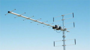
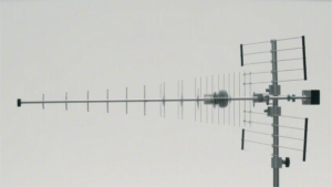
Near-field testing requires probes <1 cm in size (e.g., 1 mm H-field loops) to capture localized interference, while far-field uses horn antennas or λ/2 dipoles. A common mistake is assuming far-field behavior starts too early—real data shows near-field effects linger up to 2λ for high-Q circuits. For a 900 MHz IoT device, this means 66 cm of near-field dominance, where shielding must block both E and H fields separately.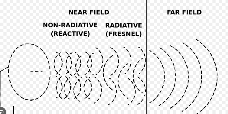
Field Strength Drop-off
The drop-off rate of electromagnetic field strength is one of the most critical differences between near-field and far-field EMI. In the near-field (within 1 wavelength (λ) of the source), field strength decays at -30 to -40 dB per decade, much faster than the far-field’s predictable -20 dB per decade (1/r²). For example, a 2.4 GHz Wi-Fi module (λ = 12.5 cm) emitting 1 W (30 dBm) produces 5 V/m at 10 cm, but only 0.5 V/m at 1 meter—a 10x drop in near-field. Meanwhile, in the far-field (beyond λ), the same signal decays to 0.05 V/m at 10 meters. Real-world measurements show that near-field probes placed <5 cm from a switching regulator detect 50-100 mV/m noise, while far-field antennas at 3 meters pick up just 1-2 mV/m.
The near-field’s rapid decay is due to reactive (non-radiative) coupling, where energy is stored in electric (E) or magnetic (H) fields rather than radiating. A 10 MHz PCB trace with 100 mA current creates an H-field that drops from 10 A/m at 1 cm to 0.1 A/m at 10 cm—a 100x reduction. In contrast, far-field radiation from a 1 GHz antenna decreases from 3 V/m at 1 meter to 0.3 V/m at 10 meters, following the 1/r² rule.
| Scenario | Frequency | Distance | Field Strength | Decay Rate |
|---|---|---|---|---|
| Near-field (H-field) | 10 MHz | 1 cm → 10 cm | 10 A/m → 0.1 A/m | -40 dB/decade |
| Near-field (E-field) | 100 MHz | 5 cm → 50 cm | 50 V/m → 0.5 V/m | -30 dB/decade |
| Far-field (radiated) | 1 GHz | 1 m → 10 m | 3 V/m → 0.3 V/m | -20 dB/decade |
If you’re placing sensitive analog circuits <5 cm from a 500 kHz buck converter, the near-field’s -30 dB/decade drop means shielding must block both E and H fields independently. A 1 mm aluminum shield might reduce E-fields by 20 dB, but H-fields require mu-metal or ferrite for similar suppression. Far-field shielding is simpler—a 0.5 mm steel enclosure typically provides 30-40 dB attenuation at 1 GHz because the wave is fully radiative.
A common mistake is assuming far-field behavior starts at λ/2π (~λ/6). In reality, high-Q resonances (e.g., RFID coils at 13.56 MHz) can extend near-field effects up to 2λ (44 meters). For compliance testing, CISPR 25 requires measurements at 3 meters, but pre-compliance scans at 1 meter often miss near-field peaks. For example, a 200 MHz clock harmonic might show 40 dBµV/m at 1 meter but 60 dBµV/m at 10 cm—a 20 dB underestimation if only far-field is checked.
Coupling Methods
Near-field and far-field EMI interact with circuits in fundamentally different ways. In the near-field (within 1 wavelength), coupling happens through direct induction—either capacitive (E-field) or inductive (H-field). For example, a 10 MHz clock trace with 3 V swing can capacitively couple 50 mV of noise into a parallel trace just 2 mm away, while the same signal induces 5 mA of ground noise through mutual inductance when loop area exceeds 1 cm². Far-field coupling is simpler—it’s radiative, with energy transfer depending on antenna efficiency. A 2.4 GHz WiFi signal at 20 dBm typically delivers -40 dBm (-80 dB coupling loss) to a poorly matched 50 Ω receiver antenna at 5 meters.
The dominant coupling mechanism depends on source impedance. High-voltage nodes (>5 V, Z > 100 Ω) like LCD drivers create E-field coupling—measurable as 1-5 pF stray capacitance between adjacent traces. A 100 MHz, 5 V signal through this capacitance injects 10-50 mA displacement current, enough to corrupt 16-bit ADC readings. Low-impedance sources (<1 Ω) like switching MOSFETs favor H-field coupling, where 50 A/µs di/dt generates 3-8 µH/m mutual inductance with nearby loops. This explains why buck converter layouts often suffer 200 mV ground bounce even with 2 mm spacing to sensitive analog traces.
Once EMI transitions to far-field, coupling becomes a function of antenna gain and path loss. A 1 GHz harmonic from a poorly filtered USB 3.0 port radiates at -10 dBm but may only induce -70 dBm in a victim antenna (60 dB path loss) at 3 meters. However, resonance effects can worsen this—a λ/4 cable at 433 MHz transforms into an efficient antenna, boosting received noise by 20 dB. Real-world data shows 90% of far-field EMI failures occur at specific frequencies where victim circuits or enclosures accidentally resonate.
For near-field, 3 mm spacing between high-speed and analog traces reduces capacitive coupling by 40 dB, while ground stitching vias every λ/20 (e.g., 1.5 mm at 1 GHz) cut inductive noise by 30 dB. Far-field solutions demand different tactics: adding 6 dB of shielding to a plastic enclosure requires 2 µm conductive coating, but the same attenuation at 10 GHz needs 1 mm aluminum. The cost difference is stark—near-field fixes often cost <0.10 per board (ferrite beads, guard traces), while far-field compliance (RF gaskets, absorbers) can add 5-20 per unit.
Measurement Setup Differences
Testing near-field vs. far-field EMI requires completely different setups—get it wrong, and you’ll miss critical failures. Near-field scans demand high-resolution probes (1-10 mm tip size) to capture localized hotspots, while far-field measurements need calibrated antennas placed at 3m/10m distances. For example, a 100 MHz clock harmonic might show 70 dBµV with a 5 mm H-field probe but only 40 dBµV/m at 3m using a biconical antenna—a 30 dB difference that could hide compliance risks. Budgets vary wildly: basic near-field kits start at 100k+.
Probe Selection & Positioning
| Parameter | Near-Field Setup | Far-Field Setup |
|---|---|---|
| Sensor Type | Miniature loops/E-field probes (1-10 mm) | Log-periodic/biconical antennas (30 cm-2m) |
| Frequency Range | DC-6 GHz (limited by probe size) | 30 MHz-18 GHz (antenna-dependent) |
| Spatial Resolution | 1-5 mm (critical for PCB traces) | N/A (averaged over λ/2 area) |
| Typical Distance | 1-50 mm from source | 1m/3m/10m (standardized) |
| Cost | 5k (handheld scanners) | 250k (chamber + equipment) |
Near-field measurements require sub-mm precision—a 2 mm probe offset can alter readings by 15 dB for high-dV/dt signals. That’s why EMI engineers use motorized XY scanners (20k) with 0.1 mm repeatability for pre-compliance testing. In contrast, far-field setups rely on antenna height sweeps (1-4m) and turntable rotation to capture worst-case radiation patterns.
Frequency & Dynamic Range Tradeoffs
Most near-field probes lose sensitivity above 3 GHz due to parasitic capacitance (typically 0.2-1 pF), limiting their use for 5G/WiFi 6E designs. Far-field antennas compensate with higher gain (5-10 dBi), but require 30 dB preamps ($3k+) to detect weak signals below -90 dBm. A 4-layer PCB might show 50 dBµV noise at 500 MHz in near-field, but radiate just 28 dBµV/m at 3m—pushing it close to FCC Class B limits (40 dBµV/m). Without both measurements, you’d miss the 12 dB margin erosion.
Ground Plane & Reflection Errors
Near-field scans often ignore ground planes, but 1 oz copper can distort H-field readings by 8-12 dB at 50 MHz. That’s why automotive EMC tests (CISPR 25) mandate 10 cm clearance from metal surfaces. Far-field chambers use anechoic foam ($200/sq.m) to suppress reflections, but even 0.5% reflectivity causes ±3 dB measurement error at 1 GHz. Pre-compliance labs often use semi-anechoic setups (60% cost savings) but accept ±5 dB uncertainty.
Time & Cost Realities
A full near-field scan of a 150×100 mm PCB takes 2-4 hours at 1 mm resolution, while far-field sweeps require 30-60 minutes per orientation. For startups, renting chamber time (800/hour) makes far-field testing 5-10x more expensive than in-house near-field scans. That’s why savvy teams use near-field data to fix 90% of issues before final far-field validation—cutting compliance retests from 5 iterations to 1-2.