A waveguide is a physical structure (e.g., metal tube or fiber optic) that confines and directs electromagnetic waves (e.g., 5G mmWave at 28GHz or optical signals) with low loss (<0.2dB/m). Guided waves refer to the propagation phenomenon itself, where energy travels along boundaries (e.g., surface acoustic waves at 1-10MHz). Waveguides enable guided waves by controlling modes (e.g., TE10 in rectangular waveguides), while guided waves can also occur naturally (e.g., seismic waves). Key difference: waveguide = hardware; guided wave = behavior.
Table of Contents
Basic Definitions
Waveguides and guided waves are fundamental concepts in RF and microwave engineering, but they’re often confused. A waveguide is a physical structure—typically a hollow metal tube or dielectric slab—that confines and directs electromagnetic waves (like radio or microwaves) with minimal loss. Common waveguide shapes include rectangular (e.g., WR-90, 22.86 mm × 10.16 mm) and circular (e.g., 50 mm diameter), operating at frequencies from 1 GHz to 300 GHz. In contrast, a guided wave refers to the actual electromagnetic wave being channeled through a medium, whether it’s a waveguide, optical fiber, or even a power line.
Waveguides are widely used in radar systems (e.g., 90% of military radars use waveguides), satellite communications (handling 10-100 kW power in high-power transmitters), and medical imaging (MRI machines often use 1.5-3.0 T magnetic fields with waveguide-fed RF coils). Guided waves, meanwhile, exist in many forms—surface acoustic waves (SAWs) in touchscreens (propagating at 3,000 m/s), optical signals in fiber optics (attenuation as low as 0.2 dB/km), and even seismic waves in oil exploration (traveling 5-8 km/s in Earth’s crust).
| Feature | Waveguide | Guided Wave |
|---|---|---|
| Physical Form | Metal/dielectric structure (e.g., aluminum, copper) | Electromagnetic or mechanical wave |
| Frequency Range | 1 GHz – 300 GHz (microwave/mmWave) | DC – THz (depends on medium) |
| Transmission Loss | 0.1 – 1.0 dB/m (depends on material) | Varies (e.g., optical fiber: 0.2 dB/km, coax: 0.5 dB/m at 1 GHz) |
| Power Handling | Up to 100 kW (high-power radar) | Limited by medium (e.g., fiber optics: ~1 W before nonlinear effects) |
| Typical Use Cases | Radar, satellite comms, particle accelerators | Fiber optics, SAW sensors, power lines |
Waveguides are engineered structures with strict dimensional tolerances—for example, a WR-112 waveguide (used in 2.6-3.95 GHz radar) must maintain an internal width of 28.5 mm ± 0.05 mm to prevent mode leakage. Guided waves, however, depend on the material properties of their medium. Optical fibers, for instance, rely on a 125 µm diameter glass core with a refractive index difference of 0.36% to keep light confined.
In terms of cost, waveguides are 10-50x more expensive than coaxial cables (e.g., 500/m vs. 10/m for RG-58 coax), but they offer lower loss at high frequencies (e.g., 0.3 dB/m at 10 GHz vs. 3 dB/m for coax). Guided waves in fiber optics, meanwhile, are cheaper for long-haul comms—deploying 10 km of single-mode fiber costs ~2,000, whereas a comparable waveguide system could exceed 50,000.
How They Carry Waves
Waveguides and guided waves transport energy in completely different ways—one is a physical highway, the other is the signal traveling on it. A rectangular waveguide (like the WR-284, 72.14 mm × 34.04 mm) carries microwaves (2.6-3.95 GHz) by reflecting them off its inner walls, with 99.9% of the energy confined inside. In contrast, a guided wave—such as a 1.55 µm optical signal in fiber—relies on total internal reflection, losing just 0.2 dB per kilometer.
The speed at which waves travel varies drastically. In a copper waveguide, a 10 GHz microwave propagates at ~95% of light speed (2.85×10⁸ m/s), while a surface acoustic wave (SAW) on a quartz crystal moves at 3,000 m/s—100,000x slower. Even power lines act as guided wave structures, transmitting 50-60 Hz AC signals at ~90% of light speed, but with 5-10% resistive loss over 100 km.
| Feature | Waveguide | Guided Wave |
|---|---|---|
| Energy Confinement | Metallic/dielectric boundaries reflect waves | Medium’s inherent properties (e.g., refractive index) |
| Propagation Speed | 0.7-0.99× light speed (depends on mode) | Varies (e.g., optical fiber: ~2×10⁸ m/s, SAW: 3,000 m/s) |
| Loss Mechanisms | Wall resistance (~0.1 dB/m at 10 GHz) | Scattering/absorption (e.g., fiber: 0.2 dB/km) |
| Frequency Limits | Cutoff frequency (e.g., WR-90: 6.56 GHz) | Depends on medium (e.g., coax: 0-100 GHz, fiber: 200 THz max) |
| Power Handling | Up to 100 kW (pulsed radar) | Fiber: ~1 W (nonlinear effects above 10 W) |
Waveguides enforce strict mode control. For example, a TE₁₀ mode in a WR-112 waveguide (28.5 mm width) only allows waves above 3.94 GHz to pass, blocking lower frequencies. Optical fibers, however, guide light via core-cladding refractive index differences—single-mode fibers use a 9 µm core with a 0.36% index contrast, while multimode fibers (50 µm core) support multiple paths but suffer modal dispersion (~3 ns/m).
Losses add up fast in real systems. A 10 m waveguide run at 24 GHz loses 1-2 dB, while a 10 km fiber link loses just 2 dB. Coaxial cables fall in between—3 dB loss per 10 m at 6 GHz—making them cheaper for short runs but impractical for high-power radar (where waveguides handle 50 kW without melting).
Common Types & Shapes
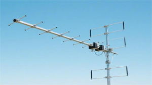
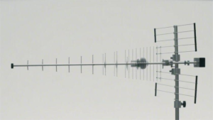
Waveguides and guided wave systems come in a variety of shapes and materials, each optimized for specific frequency ranges, power levels, and applications. The most common waveguide type is the rectangular metal waveguide, such as the WR-90 (22.86 mm × 10.16 mm), which dominates 8.2-12.4 GHz radar and satellite systems due to its low loss (0.1 dB/m) and high power handling (10+ kW). Circular waveguides (e.g., 50 mm diameter) are less common but excel in rotating radar joints and high-mode applications, supporting frequencies from 1-100 GHz with 0.05 dB/m loss in precision setups.
Dielectric waveguides, like optical fibers, use 125 µm glass strands with a 9 µm core for single-mode transmission, achieving 0.2 dB/km loss at 1550 nm wavelength. In contrast, coaxial cables—technically guided wave structures—rely on a 2-10 mm center conductor surrounded by shielding, handling DC to 100 GHz but suffering 3 dB/m loss at 6 GHz. Even power lines act as guided wave media, transmitting 50-60 Hz AC signals with 5-10% loss over 100 km due to resistive heating.
”The shape of a waveguide dictates its performance—rectangular for precision, circular for flexibility, and optical fibers for distance.”
Rectangular waveguides dominate 90% of microwave systems because their flat walls enforce TE₁₀ mode propagation, ensuring predictable cutoff frequencies (e.g., 6.56 GHz for WR-90). Their aluminum or copper construction keeps costs at 1000 per meter, while gold-plated versions (used in aerospace) push prices to $5000/m. Ridged waveguides, with internal grooves, extend bandwidth—like the WRD-180 (46 mm × 22 mm), covering 3.3-7.05 GHz but sacrificing 20% power handling due to increased surface currents.
Optical fibers come in two main types: single-mode (9 µm core, 0.36% refractive index difference) for long-haul telecom (100+ km spans) and multimode (50-62.5 µm core) for data centers (500 m max at 10 Gbps). Bend-insensitive fibers reduce loss from 0.5 dB to <0.1 dB per 90° turn, critical for FTTH installations. Meanwhile, plastic optical fiber (POF, 1 mm core) is cheaper (2/m for glass) but limited to 100 Mbps over 50 m due to high attenuation (0.5 dB/m).
Coaxial cables span from RG-58 (2.95 mm OD, 50 Ω) for 1-3 GHz lab use to semi-rigid coax (5-10 mm OD) handling 40 GHz in phased arrays. Their braided shielding blocks 90% of interference, but helical corrugated cables (like LMR-400) cut weight by 30% while maintaining 0.3 dB/m loss at 2 GHz.
Surface wave structures—like coplanar waveguides (CPW) on PCBs—route 30 GHz signals with 0.2 dB/mm loss, ideal for 5G mmWave antennas. Microstrip lines (0.5-3 mm wide traces) dominate sub-6 GHz designs, but their 50 Ω impedance tolerance (±5%) demands precise FR4 or Rogers 4350B substrates.
Where They Are Used
Waveguides and guided waves power critical systems across industries, with each technology dominating specific use cases based on their performance characteristics. Rectangular waveguides (WR-284 standard, 72.14 mm × 34.04 mm) handle 95% of military radar systems operating at 2.6-3.95 GHz, where their ability to transmit 50-100 kW pulses with just 0.1 dB/m loss makes them irreplaceable. In contrast, optical fibers carrying guided light waves form the backbone of global communications, with 99.7% of international data traffic traveling through submarine cables containing 4-8 fiber pairs, each capable of 16 Tbps (terabits per second) over 10,000 km spans.
The medical field shows another stark contrast in applications. MRI machines use waveguides operating at 64-128 MHz to deliver 1-3 kW RF power to imaging coils, while ultrasound systems rely on guided piezoelectric waves at 2-20 MHz to achieve 0.1 mm resolution in tissue imaging. Even your smartphone contains both technologies – the 5G mmWave antenna array (24-39 GHz) uses microstrip waveguide feeds, while the touchscreen detects surface acoustic waves (SAWs) traveling at 3,000 m/s with 1 mm position accuracy.
| Application | Waveguide Type | Key Parameters | Performance Advantage |
|---|---|---|---|
| Satellite Communications | Circular waveguide (50 mm diameter) | 17-21 GHz band, 0.05 dB/m loss | Survives -150°C to +120°C in space |
| Fiber Optic Networks | Single-mode fiber (9 µm core) | 1550 nm wavelength, 0.16 dB/km loss | 100 Gbps per channel over 80 km |
| Industrial Microwave Heating | WR-340 waveguide (86.36 × 43.18 mm) | 2.45 GHz, 25-100 kW power | 95% energy efficiency in food processing |
| Automotive Radar | Substrate-integrated waveguide (3 mm width) | 77-81 GHz, 0.3 dB/mm loss | Enables 1 cm resolution at 250 m range |
| Undersea Power Cables | XLPE-insulated copper (250 mm² core) | 50-60 Hz, 5% voltage drop/100 km | 800 MW transmission capacity |
In aerospace, aluminum waveguides (WR-112, 28.5 mm width) route 10-20 kW radar signals in fighter jets with 0.2 dB/m loss, while commercial airliners use dielectric waveguide antennas for 12-18 GHz satellite internet with 500 Mbps per passenger. The energy sector shows equally specialized use – power line communication (PLC) systems inject 1-30 MHz guided waves onto 138-765 kV transmission lines, achieving 1 Mbps data rates over 200 km spans without additional cabling.
5G infrastructure demonstrates how both technologies work together: base stations use waveguides for the 24-39 GHz frontend (handling 100 W per antenna), while fiber backhaul carries the baseband signal with <1 µs latency. The cost differences are dramatic – waveguide runs cost 500/m but are unavoidable at mmWave frequencies, while fiber installation runs 20,000/km but supports 100x more bandwidth.
Emerging applications continue pushing boundaries. Quantum computing labs use superconducting waveguides (niobium, 4K temperature) to preserve qubit coherence for 100+ µs, while new photonic integrated circuits guide light in 220 nm silicon channels at 200 Gbps/mm² density. Even ordinary buildings now incorporate RFID-guided surface waves in concrete (2.4 GHz, 3 m range) for structural health monitoring.
The choice between waveguides and guided wave systems ultimately comes down to frequency, power, and distance requirements. Waveguides dominate high-power RF where 1 dB loss matters more than $1,000 cost, while guided waves in fibers or cables win for long-distance or consumer-grade applications where cost per bit determines success. As frequencies keep climbing to sub-THz (100-300 GHz) for 6G and beyond, new hybrid solutions combining silicon waveguides with photonic integration are already in development to bridge these worlds.
Key Differences Listed
Waveguides and guided waves may seem similar, but their technical distinctions dictate where and how they’re used. A rectangular waveguide (WR-90, 22.86 mm × 10.16 mm) is a physical structure made of aluminum or copper, designed to carry 8.2-12.4 GHz signals with 0.1 dB/m loss, while a guided wave refers to the electromagnetic or acoustic energy itself—whether it’s light in a fiber optic (1550 nm, 0.2 dB/km loss) or vibrations in a 5 MHz ultrasonic sensor traveling at 3,000 m/s. The core difference? Waveguides are engineered pipes; guided waves are the signals flowing through them—or any other medium.
Frequency handling separates them immediately. Waveguides enforce strict cutoff frequencies—a WR-112 waveguide (28.5 mm width) won’t propagate signals below 3.94 GHz, making them useless for low-frequency radio or power transmission. Guided waves, however, adapt to their medium: 50 Hz AC power rides on copper wires, 2.4 GHz Wi-Fi propagates through air, and 200 THz infrared light guides through glass fibers. The bandwidth also differs sharply—a ridged waveguide might cover 3.3-7.05 GHz (113% relative bandwidth), while a single-mode fiber supports 1.2-1.6 µm wavelengths (25 THz bandwidth).
Power capacity is another critical divide. Waveguides handle 1-100 kW in radar systems because their metal walls prevent energy leakage, even at 20-30 kV/m field strengths. Guided waves in optical fibers, however, hit nonlinear effects above 1 W, and coax cables overheat beyond 500 W at 1 GHz. Even in power lines, guided 60 Hz waves face 5-10% resistive losses per 100 km, while waveguides in satellite transponders lose just 0.05 dB/m at 20 GHz.
Cost and installation complexity vary drastically. Deploying 10 m of WR-112 waveguide costs 5,000 due to precision machining and 0.05mm dimensional tolerances, while 10 km of single-mode fiber runs 20,000 but delivers 100 Gbps over 80 km. Coaxial cables ($10/m for RG-58) sit in the middle but suffer 3 dB/m loss at 6 GHz, making them impractical for mmWave 5G (24-39 GHz) where waveguides dominate despite their price.
Signal integrity metrics reveal more gaps. Waveguides maintain <1° phase error/m at 10 GHz, crucial for phased array radars, while optical fibers exhibit 0.1 ps/(km·nm) chromatic dispersion, limiting 400 Gbps signals to 40 km spans. Even latency differs—guided waves in PCB microstrips add 3 ps/mm delay, whereas SAW filters introduce 1 µs latency in smartphone touchscreens.
Environmental robustness splits applications further. Aerospace waveguides survive -55°C to +125°C and 50 g vibrations, while undersea fibers withstand 800 atm pressure but fail if bent below 30 mm radius. Coax cables corrode in 85% humidity unless gold-plated, but dielectric waveguides (like optical fibers) ignore EMI—a must for MRI machines with 3 T magnetic fields.
Real-World Examples
Waveguides and guided waves power technologies we use daily, often without realizing it. Your smartphone’s 5G mmWave antenna array uses waveguide-fed patch antennas (24-39 GHz) to deliver 1 Gbps speeds, while its touchscreen relies on surface acoustic waves (SAWs at 5 MHz) detecting finger positions within 0.5 mm accuracy. At larger scales, undersea fiber optic cables carrying 96% of global internet traffic utilize guided light waves (1550 nm) with just 0.16 dB/km loss, enabling 200 Tbps capacity across 10,000 km ocean spans. Meanwhile, airport radar systems depend on WR-90 waveguides (22.86×10.16 mm) to transmit 50 kW pulses at 9.4 GHz, tracking aircraft with 1.5 m range resolution in all weather conditions.
| Application | Technology Used | Key Parameters | Performance Metrics |
|---|---|---|---|
| MRI Scanners | RF waveguides (64-128 MHz) | 3-7 kW power, 1.5-3.0 T magnetic fields | 1 mm imaging resolution, 0.1 dB/m loss |
| Smart Grids | Power line communication (1-30 MHz) | 138-765 kV lines, 5% signal loss/100 km | 1 Mbps data rate over 200 km power lines |
| Autonomous Vehicles | 77 GHz substrate-integrated waveguide | 4×4 antenna array, 0.4 dB/mm loss | 3 cm resolution at 300 m range |
| FTTH Internet | Single-mode fiber (9 µm core) | 1310/1550 nm wavelengths, 0.3 dB/km splice loss | 10 Gbps symmetrical speeds to homes |
| Satellite TV | Circular waveguide (40 mm diameter) | 17.3-20.2 GHz band, 0.05 dB/m loss | 100 W SSPA output, 300+ channel capacity |
In industrial settings, 2.45 GHz waveguide systems deliver 25-100 kW microwave power to food drying tunnels, removing 60% moisture content in 30-minute cycles with 95% energy efficiency—far outperforming conventional ovens. The aerospace industry takes waveguide reliability further: fighter jet AN/APG-79 radars use pressurized WR-112 waveguides (28.5 mm width) that maintain 0.2 dB/m loss despite 15 g vibrations and -55°C to +125°C thermal cycles. Contrast this with guided wave solutions like fiber optic gyroscopes in aircraft navigation, where 500 m of coiled fiber detects Earth’s rotation with 0.01°/hr drift using 1310 nm laser light.
Telecom infrastructure showcases both technologies working together. A 5G macro base station employs waveguides for its 28 GHz AAU (64-element array) to achieve 1.5 km coverage, while fiber backhaul carries the signal with <100 µs latency to the core network. The cost differential is stark: waveguide runs cost 300/m but handle 100W RF power, while 72-core fiber cables (15/m) transport 400 Gbps per strand over 80 km without amplification.
Emerging applications push boundaries further. Quantum computers use superconducting niobium waveguides cooled to 4K (-269°C) to preserve qubit coherence for 100 µs, while photonic chips guide 200 Gbps optical signals through 220 nm silicon channels. Even civil engineering now embeds 2.4 GHz guided RF waves in concrete pillars to monitor structural health via 3 m range dielectric changes.