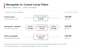
Waveguide adapters reduce avoidable signal loss by matching the electrical transition and maintaining a repeatable mechanical interface. They do not eliminate loss. Select an adapter for the operating band, waveguide mode, flange and connector, then verify insertion loss and return loss across the required sweep.
A claim such as “less than 0.1 dB loss” needs a model, frequency range, reference planes and test conditions. It is not a specification for every waveguide adapter.
Choose the right kind of adapter
| Interface change | Adapter function | Check before selection |
|---|---|---|
| Coaxial cable to waveguide | A probe, loop or other coupling structure transfers energy between the coaxial and waveguide fields | Connector type, waveguide band, orientation and power limits |
| One rectangular waveguide size to another | A shaped or stepped transition changes the guide cross-section | Common usable band, modes and measured matching |
| Different flange patterns on the same guide size | A mechanical interface change connects the mating components | Aperture alignment, flange drawings, pins and sealing faces |
| Rectangular to circular waveguide | A designed transition couples the intended modes | Mode and polarization requirements, not just aperture size |
Compare waveguide-to-coaxial adapters for cable interfaces and waveguide transitions for changes between guide sections. A rectangular-to-circular transition does not automatically provide circular polarization; that depends on the complete mode-conversion and polarizing structure.
Separate reflection from dissipative loss
An abrupt electrical discontinuity reflects part of the incident wave. Transition geometry and coupling structures are designed to control that reflection over a specified band. Conductive surfaces, dielectric supports where present, and joints can also dissipate energy. Power coupled into unwanted modes or leakage paths may reduce transmission into the desired output mode.
Return loss describes reflection; insertion loss describes transmission. With the opposite port matched, a VNA measures input reflection as S11 and forward transmission as S21. A lower VSWR or a higher positive return-loss value means less reflection.[1]
For a measured reflection coefficient magnitude |Γ|, reflected power is |Γ|² of incident power. Return loss is −20 log₁₀|Γ|, and VSWR is (1 + |Γ|)/(1 − |Γ|). The following values are calculated relationships, not Dolph product specifications.
| Return loss | VSWR, approximately | Reflected incident power | Mismatch loss, approximately |
|---|---|---|---|
| 15 dB | 1.43:1 | 3.16% | 0.140 dB |
| 20 dB | 1.22:1 | 1.00% | 0.044 dB |
| 25 dB | 1.12:1 | 0.316% | 0.014 dB |
Mismatch loss here is −10 log₁₀(1 − |Γ|²), with a matched source and the stated load reflection. It excludes dissipation. Do not add it again to an insertion-loss measurement that already includes the adapter’s reflection under the same test conditions.
For matched ports and power-normalized S-parameters, insertion loss is −20 log₁₀|S21|. A measured loss of 0.2 dB corresponds to about 95.5% transmitted incident power; 0.5 dB corresponds to about 89.1%. Those percentages do not identify how much of the missing power was reflected, dissipated or diverted into another path.
Control the interface that the RF field actually sees
Aperture steps, lateral displacement, angular misalignment and damaged mating faces can change the measured response. NIST’s work on imperfect waveguide test ports shows why interface errors must be considered in calibration and measurement, rather than assuming every joined flange is electrically ideal.[2]
Check the actual flange drawing, including locating features and sealing arrangement. The flange measurement procedure explains why a WR designation alone cannot establish mechanical compatibility. Use the specified hardware and torque; a universal torque value based only on WR size is not a reliable assembly instruction.
Support the connected cable and guide so their weight does not pull on the joint. Inspect for burrs, contamination and damage before mating. For coaxial connectors, follow the connector manufacturer’s inspection and cleaning procedure and avoid rotating the connector bodies against each other during tightening.[3]
Measure adapter loss without hiding fixture errors
- Define the DUT boundary. State whether the result covers one adapter, a pair, or the complete cable-and-waveguide assembly.
- Calibrate at the required reference planes. Use a method suited to the interfaces. A coaxial-to-waveguide DUT may require a mixed-interface calibration, characterized fixture or validated adapter-removal method.
- Sweep the full operating band. Record S11, S22 and S21; include reverse transmission and phase when required by the application.
- Check reconnection repeatability. Repeat the connection using the same assembly procedure. Investigate changes larger than the measurement uncertainty or acceptance margin.
- Save the raw data and setup. Include S-parameter files, calibration identification, frequency grid, power, IF bandwidth, temperature and DUT serial number.
Calibration reduces systematic errors but leaves residual uncertainty. Drift, noise and connector repeatability still affect the result.[4] The five-step calibration workflow includes a verification check before accepting DUT measurements.
A back-to-back pair is useful for screening, but dividing its loss by two only estimates single-adapter loss when the adapters are sufficiently equivalent and interconnecting mismatch is controlled. It does not independently establish either adapter’s performance.
Write an acceptance requirement that a supplier can test
Specify maximum insertion loss and minimum return loss across the whole required band, identifying both ports and the reference planes. Add phase or group-delay limits only when the system needs them. State whether limits apply at room temperature or over environmental conditions.
List average power and, for pulsed operation, peak power, pulse width and duty cycle. A low-power VNA sweep does not verify high-power heating or breakdown performance. Request separate evidence for those requirements.
For a model selection or quotation, send both interface drawings, the operating band, loss budget, power conditions and required test data. This lets the proposed adapter be evaluated against your assembly rather than a generic “low-loss” claim.